Question
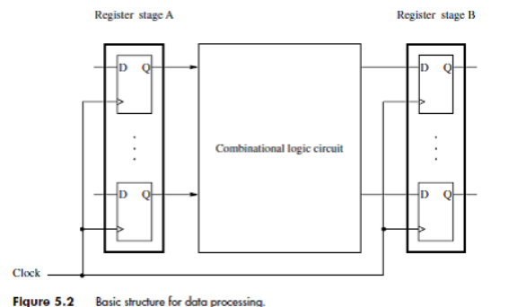
The propagation delay through the combinational circuit in Figure 5.2 is 600 Ps (picoseconds). The registers have a setup time requirement of 50 ps, and
The propagation delay through the combinational circuit in Figure 5.2 is 600 Ps (picoseconds). The registers have a setup time requirement of 50 ps, and the maximum propagation delay from the clock input to the Q outputs is 70 ps.
(a) What is the minimum clock period required for correct operation of this circuit?
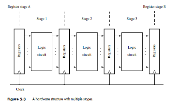
(b) Assume that the circuit is reorganized into three stages as in Figure 5.3, such that the combinational circuit in each stage has a delay of 200 ps. What is the minimum clock period in this case?
Reference of Fig.5.2


Clock Fiqure 5.2 Register stage A Combinational logic circuit Basic structure for data processing. Register stage B Register stage A Clock Stage 1 Logic circuit Stage 2 Logic circuit Figure 5.3 A hardware structure with multiple stages. Stage 3 Logic circuit Register stage B
Step by Step Solution
3.57 Rating (171 Votes )
There are 3 Steps involved in it
Step: 1
a Refer to the sequential circuit in Figure 52 in the textboo...
Get Instant Access to Expert-Tailored Solutions
See step-by-step solutions with expert insights and AI powered tools for academic success
Step: 2

Step: 3

Document Format ( 2 attachments)
6097398e269ee_27630.pdf
180 KBs PDF File
6097398e269ee_27630.docx
120 KBs Word File
Ace Your Homework with AI
Get the answers you need in no time with our AI-driven, step-by-step assistance
Get Started


