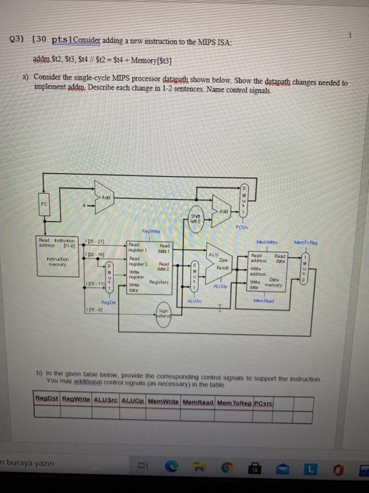
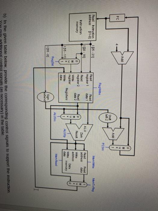
03) (30 pts 1 Consider adding a new instruction to the MIPS ISA: addo. S12, S3, St4 // $12 - $t4 + Memory[St3] a) Consider the single-cycle MIPS processor datapath shown below. Show the datapath changes needed to implement addre, Describe each change in 1-2 sentences. Name control signals. > Add PC Add PCS Pead this address 125.211 Among 01-01 19.101 das Read rege 1 Heat re ALU rustion memory Read address Wirts Read data Result regler 15.11) Register Wie ALUOO mory data Fago 06.01 sign b) in the given table below, provide the corresponding control signals to support the instruction You may additional control signals as necessary) in the table Reast Beante ALUSE ALUOR MemWrite MemRead Mem.ToRea PCs n buraya yazn TI G C - DE Add 2x PC 4- Add Shift left 2 PCSO Regte Read hstruction address 31-0) 125-21) Meminte MemToeg Read data 1 120.16) Instruction memory Read register 1 Read register 2 Vurite gister Winte data ALU Zero Result D Read data 2 Read Read address data White address Data white memory data CE - KCZO OWC 1 [15.11 Registers ALLOP ALUSE Mem Read RegDa 1116-01 Sign extend b) In the given table below, provide the corresponding control signals to support the instruction anal control signals (as necessary) in the table 03) (30 pts 1 Consider adding a new instruction to the MIPS ISA: addo. S12, S3, St4 // $12 - $t4 + Memory[St3] a) Consider the single-cycle MIPS processor datapath shown below. Show the datapath changes needed to implement addre, Describe each change in 1-2 sentences. Name control signals. > Add PC Add PCS Pead this address 125.211 Among 01-01 19.101 das Read rege 1 Heat re ALU rustion memory Read address Wirts Read data Result regler 15.11) Register Wie ALUOO mory data Fago 06.01 sign b) in the given table below, provide the corresponding control signals to support the instruction You may additional control signals as necessary) in the table Reast Beante ALUSE ALUOR MemWrite MemRead Mem.ToRea PCs n buraya yazn TI G C - DE Add 2x PC 4- Add Shift left 2 PCSO Regte Read hstruction address 31-0) 125-21) Meminte MemToeg Read data 1 120.16) Instruction memory Read register 1 Read register 2 Vurite gister Winte data ALU Zero Result D Read data 2 Read Read address data White address Data white memory data CE - KCZO OWC 1 [15.11 Registers ALLOP ALUSE Mem Read RegDa 1116-01 Sign extend b) In the given table below, provide the corresponding control signals to support the instruction anal control signals (as necessary) in the table


