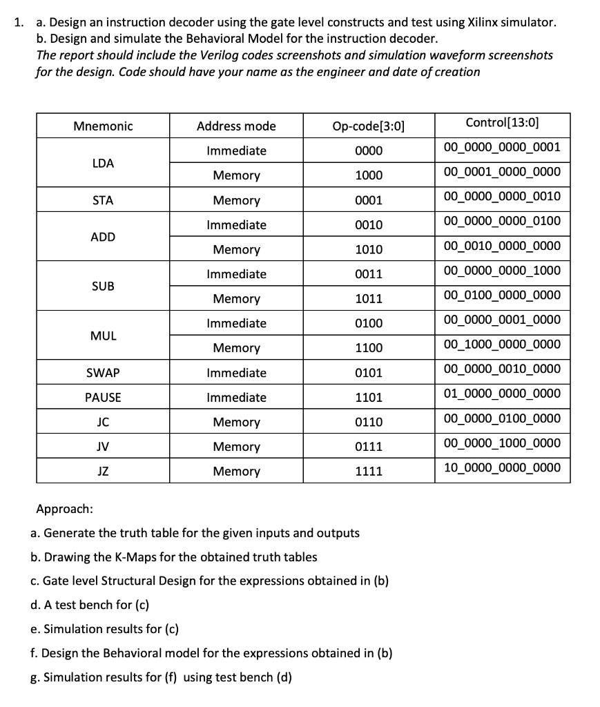
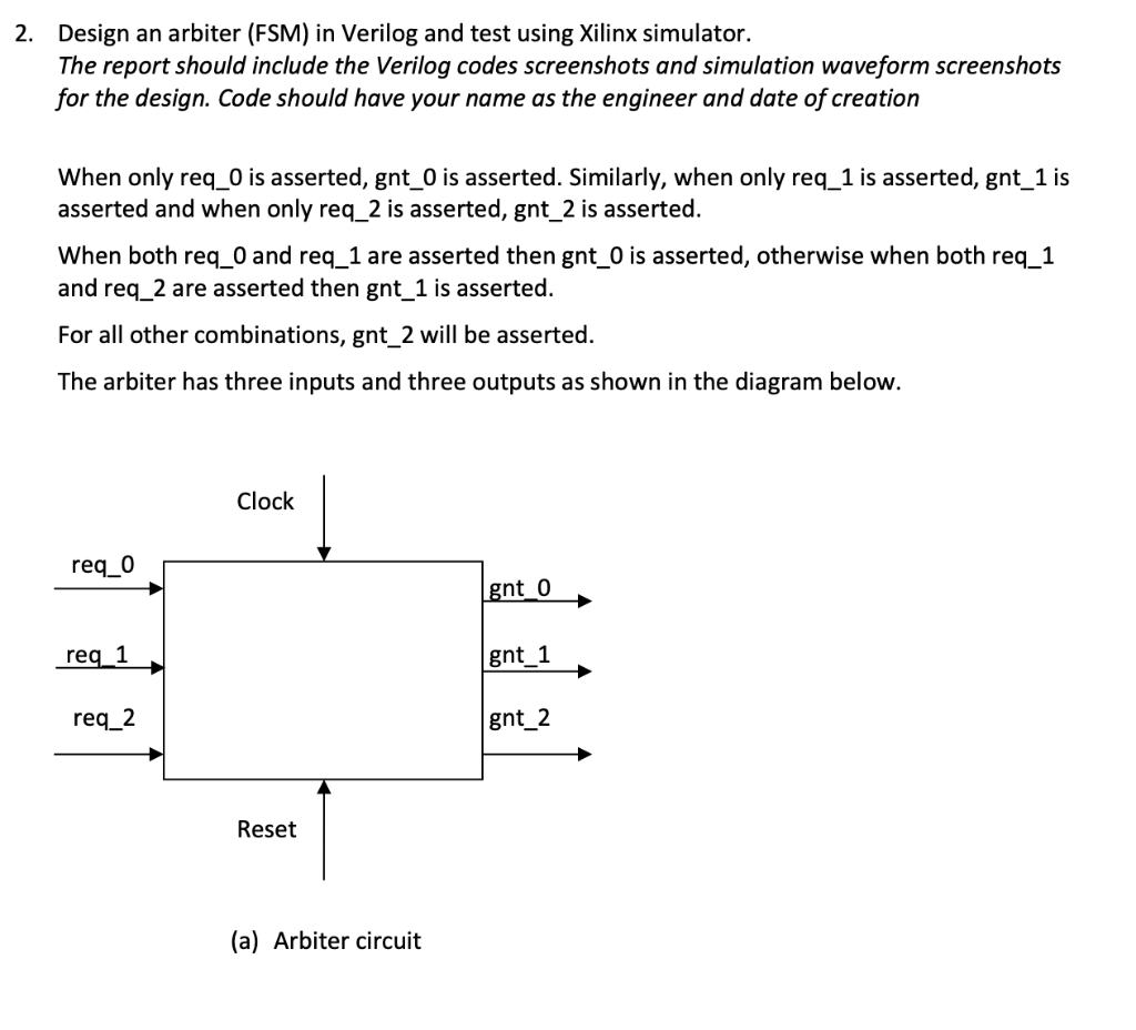
1. a. Design an instruction decoder using the gate level constructs and test using Xilinx simulator. b. Design and simulate the Behavioral Model for the instruction decoder. The report should include the Verilog codes screenshots and simulation waveform screenshots for the design. Code should have your name as the engineer and date of creation Mnemonic Address mode Op-code[3:0) Immediate 0000 LDA Memory 1000 STA Memory 0001 Immediate 0010 ADD Memory 1010 Immediate 0011 SUB Memory 1011 Control[13:0) 00_0000_0000_0001 00_0001_0000_0000 00_0000_0000_0010 00_0000_0000_0100 00_0010_0000_0000 00_0000_0000_1000 00_0100_0000_0000 00_0000_0001_0000 00_1000_0000_0000 00_0000_0010_0000 01_0000_0000_0000 00_0000_0100_0000 00_0000_1000_0000 10_0000_0000_0000 Immediate 0100 MUL Memory 1100 SWAP Immediate 0101 PAUSE Immediate 1101 JC Memory 0110 JV Memory 0111 JZ Memory 1111 Approach: a. Generate the truth table for the given inputs and outputs b. Drawing the K-Maps for the obtained truth tables c. Gate level Structural Design for the expressions obtained in (b) d. A test bench for (c) e. Simulation results for (c) f. Design the Behavioral model for the expressions obtained in (b) g. Simulation results for (f) using test bench (d) 2. Design an arbiter (FSM) in Verilog and test using Xilinx simulator. The report should include the Verilog codes screenshots and simulation waveform screenshots for the design. Code should have your name as the engineer and date of creation When only req_0 is asserted, gnt_0 is asserted. Similarly, when only req_1 is asserted, gnt_1 is asserted and when only req_2 is asserted, gnt_2 is asserted. When both req_0 and req_1 are asserted then gnt_0 is asserted, otherwise when both req_1 and req_2 are asserted then gnt_1 is asserted. For all other combinations, gnt_2 will be asserted. The arbiter has three inputs and three outputs as shown in the diagram below. Clock req_0 gnt_o reg_1 gnt_1 req_2 gnt_2 Reset (a) Arbiter circuit 1. a. Design an instruction decoder using the gate level constructs and test using Xilinx simulator. b. Design and simulate the Behavioral Model for the instruction decoder. The report should include the Verilog codes screenshots and simulation waveform screenshots for the design. Code should have your name as the engineer and date of creation Mnemonic Address mode Op-code[3:0) Immediate 0000 LDA Memory 1000 STA Memory 0001 Immediate 0010 ADD Memory 1010 Immediate 0011 SUB Memory 1011 Control[13:0) 00_0000_0000_0001 00_0001_0000_0000 00_0000_0000_0010 00_0000_0000_0100 00_0010_0000_0000 00_0000_0000_1000 00_0100_0000_0000 00_0000_0001_0000 00_1000_0000_0000 00_0000_0010_0000 01_0000_0000_0000 00_0000_0100_0000 00_0000_1000_0000 10_0000_0000_0000 Immediate 0100 MUL Memory 1100 SWAP Immediate 0101 PAUSE Immediate 1101 JC Memory 0110 JV Memory 0111 JZ Memory 1111 Approach: a. Generate the truth table for the given inputs and outputs b. Drawing the K-Maps for the obtained truth tables c. Gate level Structural Design for the expressions obtained in (b) d. A test bench for (c) e. Simulation results for (c) f. Design the Behavioral model for the expressions obtained in (b) g. Simulation results for (f) using test bench (d) 2. Design an arbiter (FSM) in Verilog and test using Xilinx simulator. The report should include the Verilog codes screenshots and simulation waveform screenshots for the design. Code should have your name as the engineer and date of creation When only req_0 is asserted, gnt_0 is asserted. Similarly, when only req_1 is asserted, gnt_1 is asserted and when only req_2 is asserted, gnt_2 is asserted. When both req_0 and req_1 are asserted then gnt_0 is asserted, otherwise when both req_1 and req_2 are asserted then gnt_1 is asserted. For all other combinations, gnt_2 will be asserted. The arbiter has three inputs and three outputs as shown in the diagram below. Clock req_0 gnt_o reg_1 gnt_1 req_2 gnt_2 Reset (a) Arbiter circuit