

Answered step by step
Verified Expert Solution
Question
1 Approved Answer
1 . Create the VHDL files provided by in appendix A adding them to your VHDL project ( Remember you need only one project for
Create the VHDL files provided by in appendix A adding them to your VHDL
project Remember you need only one project for the entire course
Fully comment the code provided in appendices A and B
Obtain the RTL schematics of the Instruction Fetch stage, and each of its
components. Write down the differences between these schematics and the ones
in Figure
Translate the code shown in the listing to binary using the basic instruction
formats shown in Figure and fill the two leftmost columns of Table with the
register letters u v w x y resolved to their equivalent numbers as explained
below.
Listing : Assembly Code
start: lw RuR
lw RvR
add Rw Ru Rv
sub Rx Ru Rv
sw RxR
slt Ry Ru Rv
beq Ru Ru start
where u is the first nonzero digit of your id number, v is the second nonzero digit of
your id number, w is the third nonzero digit of your id number, and x is the fourth non
zero digit of your id number, and y is a random number between and
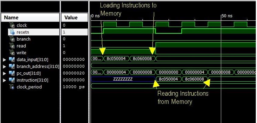
Create a test bench file and run a simulation showing the operation of the instruction
fetch stage. You must first load your program Listing binary instructions obtained
in the previous step, into the instruction memory in order to have instructions to fetch.
To do that follow the sample test bench file shown in appendix B Your simulation
should look similar to the one in Figure only that it should include all instructions to
be loaded and fetched. Explain the results of that simulation using annotations on the
timing diagram. Figure : IF simulation timing diagram for instructions. Source: Generated using Xilinx Vivado
Table : Instructions
Instructions loaded to IM Output Port Signals from Simulation
Assembly Hexadecimal Clock Cycle Instruction hex PChex
Appendix: A: Code
Listing A: Instruction Fetch Stage Code
use IEEE.STDLOGICALL;
use IEEE.STDLOGICARITH.ALL;
use IEEE.STDLOGICUNSIGNED.ALL;
entity IFetch is
Port clock, Resetn, branch : in STDLOGIC;
read, write : in STDLOGIC;
PCout, PCmas : out STDLOGICVECTOR downto ;
datainput: in STDLOGICVECTOR downto ;
branchaddress : in STDLOGICVECTOR downto ;
Instruction: out STDLOGICVECTOR downto ;
end IFetch;
architecture Behavioral of IFetch is
signal PCin PC PCplus : stdlogicvector downto
:others;
component memmodule is For N words
genericN: integer:;
Port clock: in stdlogic;
address : in STDLOGICVECTOR N downto ;
datainput: in STDLOGICVECTOR downto ;
dataoutput: out STDLOGICVECTOR downto ;
Read, write: in STDLOGIC;
end component;
component muxbits is
port
input : in stdlogicvector downto ;
input : in stdlogicvector downto ;
output : out stdlogicvector downto ;
control : in stdlogic;
end component;
component registron is
Generic N: integer:;
Port clock, enable : in stdlogic;
D : in STDLOGICVECTOR N downto ;
Q : out STDLOGICVECTOR N downto ;
Resetn : in STDLOGIC;
end component;
begin
PCoutPC;
InstructionMemory: memmodule generic mapN
port map clock,
PC downto
datainput,
Instruction,
read,
write;
PCreg: registron generic map N
port map clock,
resetn,
PCin
PC
resetn;
branchmux : muxbits port map PCplus
branchaddress,
PCin
branch;
PCplusPC;
PCmasPCplus;
end Behavioral;
Memory Module
Listing A: Memory Module Code
library IEEE;
use IEEE.STDLOGICALL;
use IEEE.STDLOGICARITH.ALL;
use IEEE.STDLOGICUNSIGNED.ALL;
entity memmodule is
genericN: integer:; For N bits
Port clock: in stdlogic;
address : in STDLOGICVECTOR N downto ;
datainput: in STDLOGICVECTOR downto ;
dataoutput: out STDLOGICVECTOR downto ;
Read, write: in STDLOGIC;
end memmodule;
architecture Behavioral of memmodule is
type mem is array N downto of stdlogicvector
downto ;
signal mem : mem:othersothers;
signal mem : mem:othersothers;
signal mem : mem:othersothers;
signal mem : mem:othersothers;
signal addressinternal :integer range to N;
signal dataoutint :STDLOGICVECTOR downto ;
begin
addressinternalconvintegeraddressN downto ;
dataoutputdataoutint;
dataoutint memaddressinternal &
memaddressin
Step by Step Solution
There are 3 Steps involved in it
Step: 1

Get Instant Access to Expert-Tailored Solutions
See step-by-step solutions with expert insights and AI powered tools for academic success
Step: 2

Step: 3
Ace Your Homework with AI
Get the answers you need in no time with our AI-driven, step-by-step assistance
Get Started
Relational Database And SQL
Authors: Lucy Scott
3rd Edition
1087899699, 978-1087899695