Answered step by step
Verified Expert Solution
Question
1 Approved Answer
1. Introduction In this lab, we are going to design a simple digital system. In addition, we will try to minimize the logical circuit by
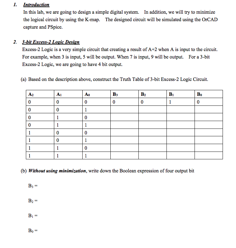
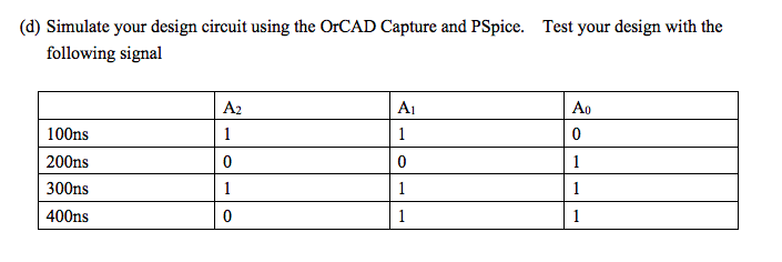
1. Introduction In this lab, we are going to design a simple digital system. In addition, we will try to minimize the logical circuit by using the K-map. The designed circuit will be simulated using the OrCAD capture and PSpice. 2. 3-bit Excess-2 Logic Design Excess-2 Logic is a very simple circuit that creating a result of A+2 when A is input to the circuit. For example, when 3 is input, 5 will be output. When 7 is input, 9 will be output. For a 3-bit Excess-2 Logic, we are going to have 4 bit output. (a) Based on the description above, construct the Truth Table of 3-bit Excess-2 Logic Circuit. A2 Ao B1 A 0 B3 0 B2 0 0 1 0 0 0 1 0 0 1 0 1 0 1 1 0 0 0 1 1 0 1 1 1 1 1 (b) Without using minimization, write down the Boolean expression of four output bit B3 B2- B = Bo= (d) Simulate your design circuit using the OrCAD Capture and PSpice. Test your design with the following signal A2 1 A1 1 100ns A0 0 1 1 200ns 0 1 0 1 300ns 400ns 0 1 1
Step by Step Solution
There are 3 Steps involved in it
Step: 1
Get Instant Access to Expert-Tailored Solutions
See step-by-step solutions with expert insights and AI powered tools for academic success
Step: 2
Step: 3
Ace Your Homework with AI
Get the answers you need in no time with our AI-driven, step-by-step assistance
Get Started