

Question: 1. Referring to the data in Exhibit 5, is the process capable of meeting GME's internal wire-bond strength requirement of at least seven grams? Use
1. Referring to the data in Exhibit 5, is the process capable of meeting GME's internal wire-bond strength requirement of at least seven grams? Use Cpk in explaining your answer.
2. Referring to the data in Exhibit 5, is the wire-bonding process in control? What implications does your determination of whether the process is in control or out of control pose for assessing the new machine's capability to meet the wire-bond strength requirement?
3. In general, what are the options for improving the capability of a process? Which of these options would you recommend Regan focus on? Why?
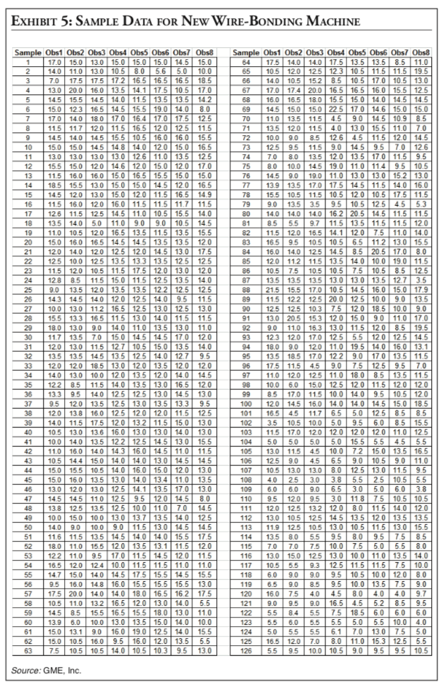
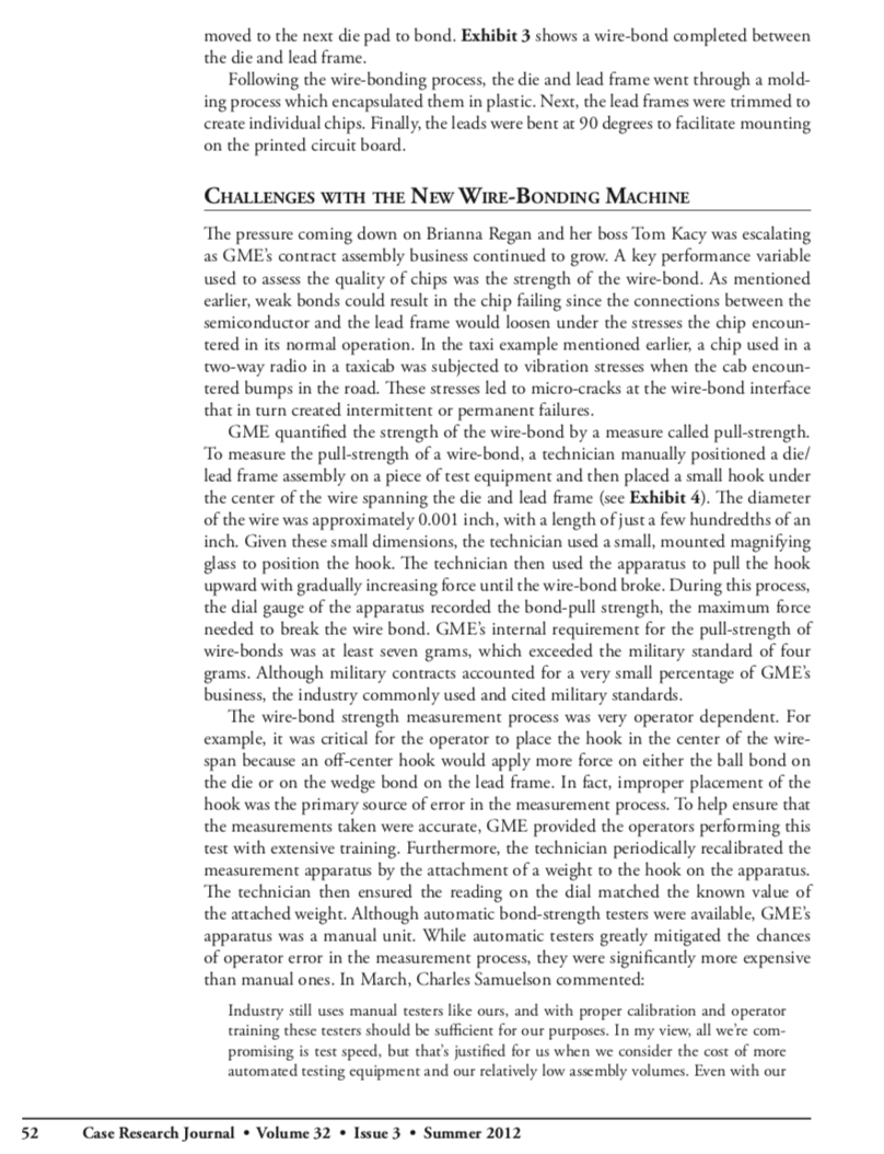
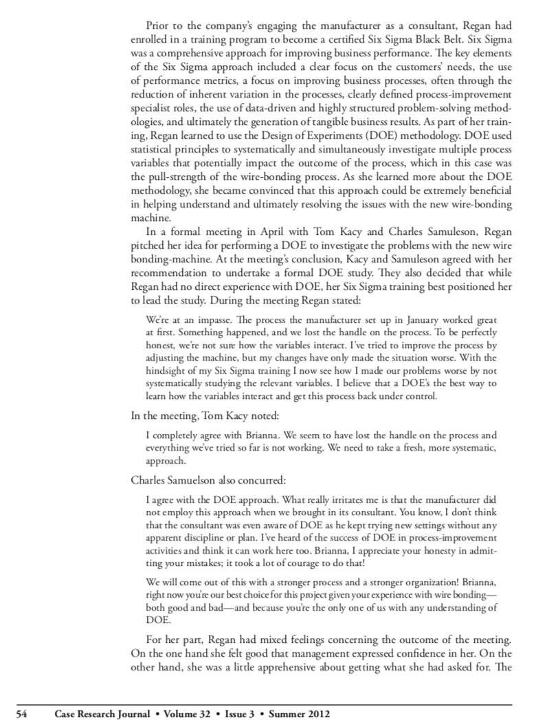
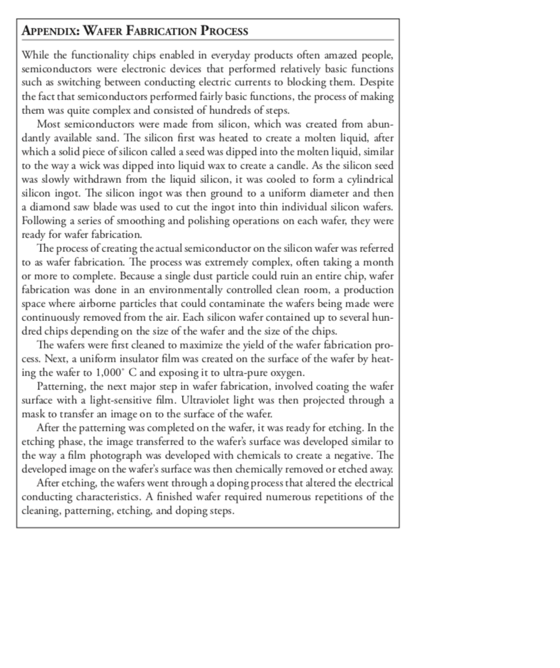
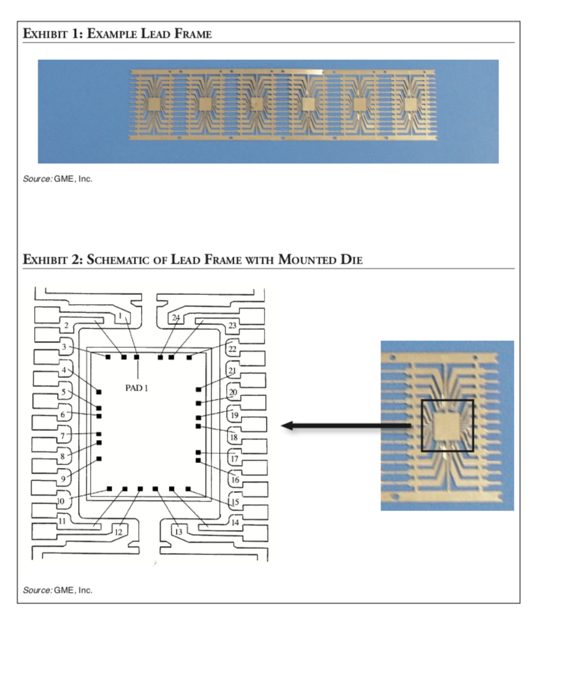
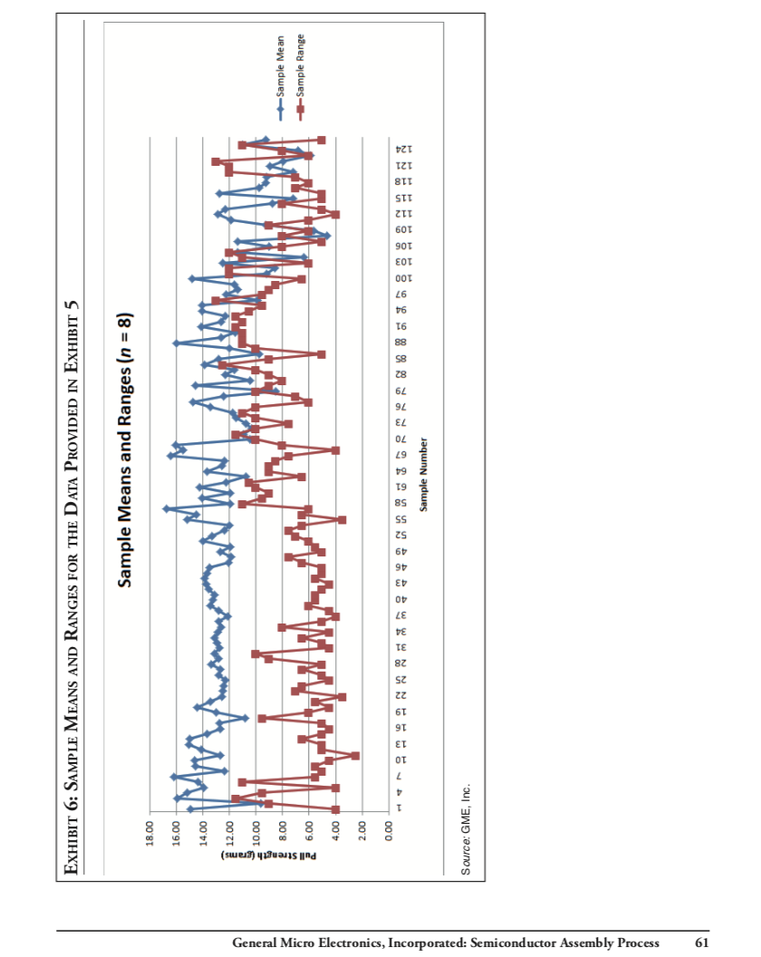
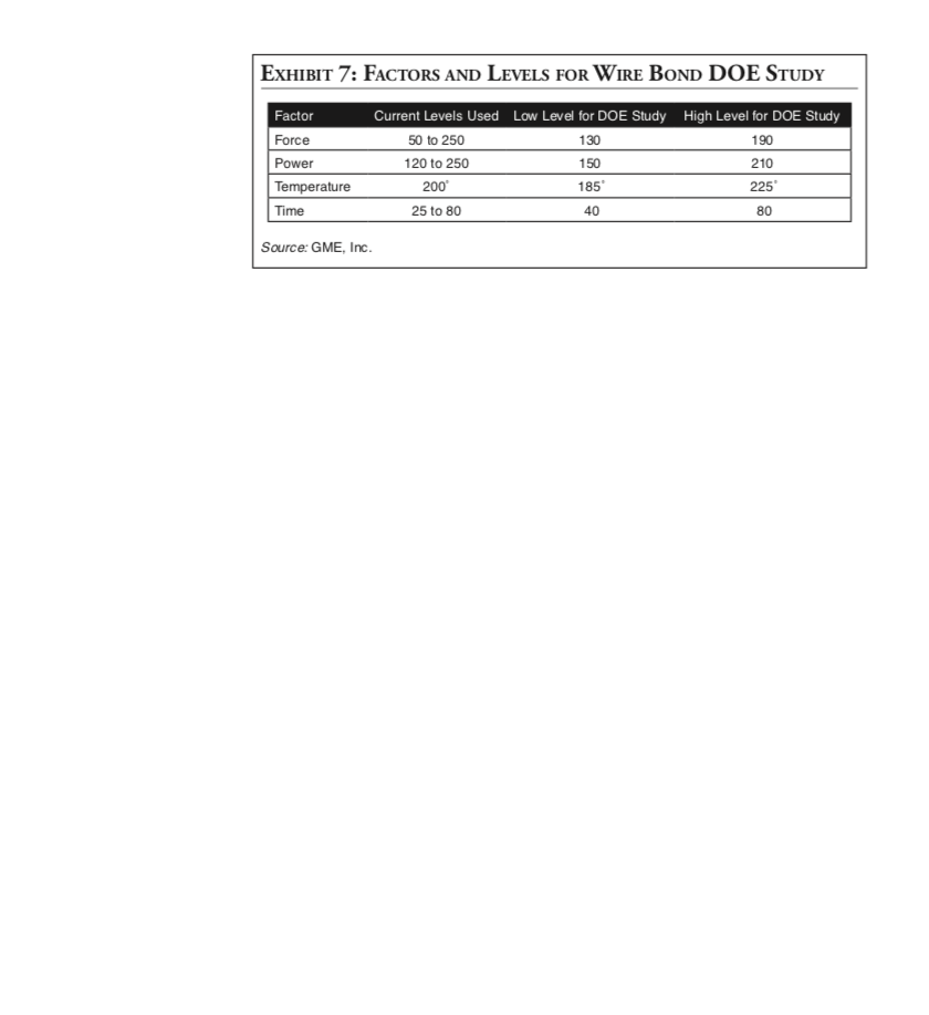
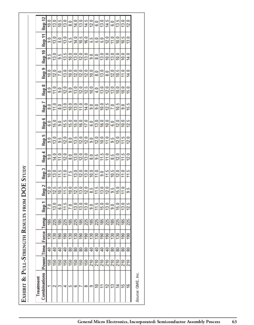
EXHIBIT 5: SAMPLE DATA FOR NEW WIRE-BONDING MACHINE Sample Obs1 Obs2 Obs3 Obs4 Obs5 Obs6 Obs7 Obs8 Sample Obs1 Obs2 Obs3 Obs4 Obs5 Obs6 Obs7 Obs8 17.0 15.0 13.0 15.0 15.0 15.0 14.5 15.0 64 17.5 14.0 14.0 17.5 13.5 13.5 8.5 11.0 2 140 11.0 13.0 10.5 8.0 5.6 5.0 10.0 65 10.5 12.0 12.5 12 3 10.5 11.5 11.5 19.5 3 7.0 17.5 17.5 17.2 16.5 16.5 16.5 18.5 66 14.0 10.5 15.2 8.5 10.5 17.0 10.5 13.0 13.0 20.0 16.0 13.5 14.1 17.5 10.5 17.0 67 17.0 17.4 20.0 16.5 16.5 16.0 15.5 12.5 5 145 15 5 14.5 14.0 11.5 13.5 13.5 14.2 68 16.0 16.5 18.0 15.5 15.0 14.0 14.5 14.5 6 15.0 123 16.5 14.5 15.5 19.0 14.0 8.0 69 14.5 15.0 15.0 22.5 17.0 14.6 15.0 15.0 7 17.0 140 180 17.0 16.4 17.0 17.5 12.5 70 11.0 13.5 11.5 4.5 9.0 14.5 10.9 8.5 8 11.5 11.7 120 11.5 16.5 12.0 12.5 11.5 71 13.5 12.0 11.5 4.0 13.0 15.5 11.0 7.0 9 14.5 140 145 15.5 10.5 16.0 16.0 15.5 72 10.0 9.0 8.5 12.6 4.5 11.5 120 14.5 10 15.0 15.0 145 14.8 14.0 12.0 15.0 16.5 73 12.5 9.5 11.5 9.0 14.5 9.5 7.0 12.6 11 13.0 13.0 13.0 13.0 12.6 11.0 13.5 12.5 74 7.0 8.0 13.5 12.0 13.5 17.0 11.5 9.5 12 15.5 150 120 14.6 120 15.0 120 17.0 75 8.0 10.0 145 19.0 11.0 114 95 10.5 13 11.5 16.0 16.0 15.0 16.5 15.5 15.0 15.0 76 14.5 9.0 19.0 11.0 13.0 13.0 15.2 13.0 14 185 15.5 13.0 15.0 15.0 14.5 12.0 16.5 77 13.9 13.5 17.0 17.5 14.5 11.5 14.0 16.0 15 145 120 13.0 15.0 120 11.5 16.5 14.9 78 15.5 10.5 11.5 10.5 12.0 10.5 17.5 11.5 16 11.5 160 120 16.0 11.5 11.5 11.7 11.5 79 9.0 13.5 3.5 9.5 10.5 4.5 5.3 17 126 11.5 125 14.5 11.0 10.5 15.5 14.0 80 14.0 14.0 14.0 16.2 20.5 14.5 1 11.5 11.5 18 135 140 5.0 11.0 9.0 9.0 10.5 14.5 81 8.5 5.5 9.7 11.5 13.5 11.5 11.5 12.0 19 11.0 10.5 120 16.5 13.5 11.5 13.5 15.5 82 11.5 12.0 16.5 14.1 12.0 7.5 11.0 14.0 20 150 160 165 14.5 14.5 13.5 13.5 12.0 83 16.5 9.5 10.5 10.5 6.5 112 13.0 15.5 21 120 14.0 120 12.5 12.0 14.5 13.0 17.5 84 16.0 14.0 12.5 14.5 8.5 20.5 17.0 8.0 22 125 10.0 125 13.5 13.3 13.5 12.5 125 85 120 11.2 11.5 13.5 14.0 10.0 19.0 11.5 23 11.5 120 10.5 11.5 17.5 12.0 13.0 12.0 86 10.5 7.5 10.5 10.5 7.5 10.5 8.5 12.5 24 128 85 11.5 15.0 11.5 125 13.5 14.0 87 13.5 13.5 13.5 13.0 13.0 13.5 12.7 3.5 25 9.0 13.5 12.0 13.5 13.5 12.2 12.5 12.5 88 21.5 15.5 17.0 10.5 14.5 16.0 15.0 17.9 26 143 145 140 120 125 14.0 9.5 11.5 89 11.5 12.2 125 20.0 12 5 10.0 9.0 13.5 27 10.0 13.0 11.2 16.5 12.5 13.0 12.5 13.0 90 12.5 12.5 10.3 7.5 12.0 18.5 10.0 9.0 28 155 13 3 165 11.5 13.0 14.0 11.5 11.5 91 13.0 20.5 153 12.0 15.0 9.0 11.0 17.0 29 18.0 13.0 9.0 14.0 11.0 13.5 13.0 11.0 92 9.0 11.0 16.3 13.0 11.5 12.0 8.5 19.5 30 11.7 135 7.0 15.0 14.5 14.5 17.0 12.0 93 12.3 12.0 17.0 12.5 5.5 12.0 12.5 14.5 31 120 13.0 11.5 12.7 10.5 15.0 13.5 14.0 94 18.0 9.0 12.0 11.0 19.5 14.0 16.0 13.1 32 135 135 145 13.5 12 5 14.0 12.7 9.5 95 13.5 18.5 17.0 12.2 9.0 17.0 13.5 11.5 33 120 120 18.5 13.0 12.0 13.5 12.0 120 96 17.5 11.5 4.5 9.0 7.5 125 9.5 7.0 34 140 13.0 10.0 12.0 13.5 12.0 14.0 14.5 97 11.0 12.0 125 11.0 18.0 8.5 13.5 11.5 35 122 8.5 11.5 14.0 13.5 13.0 16.5 120 98 10.0 6.0 15.0 12.5 12 0 11.5 120 120 133 95 140 12 5 12 5 13.0 14.5 1 99 8.5 17.0 11.5 10.0 14.0 9.5 10.5 12.0 37 9.5 120 13.5 12.5 13.0 13.5 13.3 9.5 100 12.0 14.5 16.0 14.0 14.0 14.5 15.0 18.5 38 120 13.8 16.0 12 5 12.0 12.0 11.5 12.5 101 16.5 4.5 11.7 6.5 5.0 12 5 85 85 39 140 11.5 17.5 12.0 13.2 11.5 15.0 13.0 102 3.5 10.5 10.0 5.0 9.5 6.0 8.5 15.5 40 10.5 13.0 13.6 16.0 13.0 13.0 14.0 13.0 103 11.5 17.0 12.0 12.0 12.0 12.0 11.0 12.5 41 10.0 140 13.5 12 2 12.5 14.5 13.0 15.5 104 5.0 5.0 5.0 5.0 15.5 5.5 4.5 5.5 42 11.0 16.0 14.0 14.3 16.0 14.5 11.0 11.5 105 13.0 11.5 4.5 10.0 7.2 15.0 13.5 16.5 43 10.5 14.4 15.0 14.0 14.0 13.0 14.5 14.5 106 12.5 9.0 4.5 6.5 9.0 10.5 9.0 11.0 44 15.0 15.5 10.5 14.0 16.0 15.0 12.0 13.0 107 10.5 13.0 13.0 8.0 12 5 13.0 11.5 9.5 45 15.0 16.0 13.5 13.0 14.0 13.4 11.0 13.5 108 4.0 25 3.0 3.8 5.5 25 10.5 5.5 46 13.0 120 13.0 12 5 14.1 13.5 17.0 13.0 109 6.0 6.0 9.0 6.5 3.0 5.0 6.0 3.8 47 145 145 11.0 125 9.5 120 14.5 8.0 110 9.5 120 95 3 3.0 11.8 7.5 10.5 10.5 48 13.8 125 135 12 5 10.0 11.0 7.0 14.5 111 12.0 12.5 13.2 12.0 8.0 11.5 14.0 12.0 49 10.0 15.0 10.0 13.0 13.7 13.5 14.0 125 112 13.0 10.5 125 14.5 13.5 12 0 13.5 13.5 50 14.0 9.0 10.0 9.0 11.5 13.0 14.5 14.5 113 11.9 12.5 10.5 13.0 10.5 11.5 13.0 15.5 51 11.6 11.5 13.5 14.5 14.0 14.0 15.5 17.5 114 13.5 8.0 5.5 9.5 8.0 9.5 7.5 8.5 52 180 11.0 15.5 120 13.5 13.1 11.5 12.0 115 7.0 7.0 7.5 10.0 7.5 5.0 5.5 8.0 53 122 11.0 9.5 17.0 11.5 14.5 12.0 11.5 116 13.0 15.0 125 13.0 10.0 11.0 13.5 14.0 54 16.5 120 124 10.0 11.5 11.5 11.0 11.0 117 10.5 5.5 9.3 12.5 11.5 11.5 7.5 10.0 55 147 15.0 140 14.5 17.5 15.5 14.5 15.5 118 6.0 9.0 9.5 10.5 10.0 12.0 8.0 56 9.5 16.0 14.8 16.0 15.5 15.5 15.5 1 119 6.5 9.0 8.5 9.5 10.0 13.5 7.5 9.0 57 17.5 20.0 140 14.0 18.0 16.5 16.2 1 120 16.0 7.5 4.0 4.5 8.0 4.0 4.0 9.7 58 10.5 11.0 13.2 16.5 12.0 13.0 14.0 5.5 121 9.0 9.5 9.0 16.5 4.5 5.2 85 9.5 59 145 85 155 16.5 15.5 18.0 13.0 11.0 122 5.5 8.4 5.5 7.5 18.5 6.0 6.0 6.0 60 13.9 6.0 10.0 13.0 13.5 15.0 14.0 10.0 123 5.5 6.0 5.5 5.5 5.0 5.5 10.0 4.0 61 150 131 90 16.0 19.0 125 14.0 15.5 124 5.0 5.5 5.5 6.1 7.0 13.0 7.5 5.0 62 15.0 10.5 16.0 9.5 16.0 12.0 13.5 5.5 125 16.5 12.0 7.0 8.0 11.0 15.3 12.5 5.5 63 7.5 10 5 10.5 14.0 10.5 103 95 13.0 126 55 95 10.0 10.5 90 95 95 10.5 Source: GME, Inc.ch American General Micro Electronics, Incorporated: ssociation, Inc Semiconductor Assembly Process Scott M. Shafer, Wake Forest University Charles Volk, Effective Business Solutions GENERAL MICRO ELECTRONICS, INCORPORATED: SEMICONDUCTOR ASSEMBLY PROCESS Having just left a tense meeting with Tom Kacy (her boss) and Charles Samuelson (Kacy's boss), Brianna Regan, process engineer at General Micro Electronics (GME), was sitting in her office. She shifted her gaze from the data she was studying in the Excel spreadsheet to the sample semiconductor chips scattered on her desk. She tapped nervously with her pencil and stared at the chips. She was reflecting on what the data was saying and thinking about what her recommendations were going to be to turn around the performance of the new automated wire-bonder machine used in GME's assembly operation. The company had purchased the new machine and had it all set up by the begin- ning of January. It was now May, and Regan was becoming increasingly frustrated with her inability to get control over the machine. She knew that if the new machine's performance continued to deteriorate, she would soon be getting the type of attention from senior management she would prefer to avoid. GME purchased the new wire-bonder machine in part to support the company's contract assembly business which was growing three times faster than the company's proprietary semiconductor business. From its initial installation in January through February, the new machine performed well in terms of the wire-bond strength. How- ever, beginning in March, its performance became more erratic, although still accept- able. By April, the machine's performance had grown more and more erratic to the point that it was finally deemed unacceptable to the operations managers at GME. Regan herself was becoming increasingly frustrated with the machine's inability to Copyright @ 2012 by the Case Research Journal and by Scott M. Shafer and Charles Volk. In submitting this case to the Case Research Journal for widespread distribution in print and electronic media, I (we) certify that it is original work, based on real events in a real organization. It has not been published and is not under review elsewhere. Copyright holders have given written permission for the use of any material not permitted by the "Fair Use Doctrine." The host organization has assigned a release authorizing the publication of all information gathered with understandings of confidentiality. The authors are grateful to Dr. Deborah Ertington, the editor of the Case Research Journal, and three anonymous reviewers who gave invaluable advice and suggestions for improving this case and to John Waltman for his copy editing expertise. This case was developed for the sole purpose of providing mare- rial for course analysis and class discussion. It is not intended to illustrate either effective or ineffective handling of a managerial situation. All characters, data, and events are real, but names of people, organi- zations, and dates have been disguised. General Micro Electronics, Incorporated: Semiconductor Assembly Process 49meet GME's internal standards. In fact, the continuous adjustments she had made on the machine in an effort to rectify the situation during the intervening months seemed to be making the situation worse. The need to improve the performance of the new wire-bonding machine was becom- ing critical as overtime costs were mounting and the operation would soon constrain the growth of GME's contract assembly business. Tom Kacy, manufacturing manager and Regan's boss, reflected this at the meeting earlier that day when he told her. Brianna, we've got to correct the problems with the new machine ASAP! We're sched- uling overtime on our existing outdated wire-bonding machines but they're very close to full utilization. We really need the capacity of the new machine. The wire-bond strength was an important quality dimension for semiconductor chips. In particular, when chips were subjected during use to such external stresses as vibration and heat, the wire-bonds could loosen, causing the chips to fail. Given that the chips GME supplied to its customers represented a small percentage of the total unit cost of the products they were used in, GME's customers became very disgruntled when their products failed as a result of an inexpensive defective chip. In one instance, a $500 two-way radio used in a taxi cab failed because a $2.00 chip was defective. At that same meeting, Charles Samuelson, VP of Operations, expressed his concern: Without additional capacity we won't be able to meet our promised delivery dates. We also can't afford to compromise on the quality our customers expect. Historically, fewer than 10 chips out of every million we ship have been returned because of quality problems. THE SEMICONDUCTOR INDUSTRY Semiconductors (aka integrated circuits, ICs, and chips) had become a ubiquitous part of life and had transformed the way people worked and lived. They were the heart of most electronic products and greatly enhanced the functionality of numerous other products. Imagine how different life would have been over the last decade without cell phones, personal computers, GPS devices, and video games. Likewise, consider how semiconductors enhanced the functionality of numerous products including automo- biles, medical equipment, TVs, cameras, dishwashers, and hearing aids, just to name a few. Beyond transforming our lives, the semiconductor industry played a critical role in the United States' economy. Semiconductors were a major category of U.S. exports, and U.S. sales accounted for almost half of worldwide sales. The industry was a sig- nificant source of employment in the U.S., both directly and indirectly as the enabling technology for other products. GENERAL MICRO ELECTRONICS, INC. Founded in 1968, GME designed and supplied a range of low-power analog, digi- tal, and mixed signal semiconductors used to support communication applications. Its headquarters were in the UK, and it had operations in the U.S., Germany, and Singapore. GME operated in four major segments: wireless, memory management, wire line telecommunications, and networking. The wireless portion of its business accounted 50 Case Research Journal . Volume 32 . Issue 3 . Summer 2012for 45 percent of sales and provided chips for voice, data, signaling, and radio frequency applications. Memory management applications accounted for an additional 36 percent of sales. GME's sales were approximately $30 million. GME was what industry experts called a fabless (literally "without fabrication") semiconductor company, meaning that it performed the assembly and test operations of its semiconductors in-house but out- sourced the production of the silicon wafers (a process discussed in more detail in the Appendix). More specifically, GME's primary business activity was contract assembly. As a contract assembler, it received semiconductor wafers, or chips, from its customers, assembled them into packages, and electrically tested the finished packages. GME's SEMICONDUCTOR ASSEMBLY PROCESS As a fabless semiconductor firm, GME outsourced wafer fabrication (the Appendix provides additional details of the wafer-fabrication process). When a completed wafer arrived, GME's technicians first tested each semiconductor or die within the wafer and recorded the locations of defective dies within the wafer. Next the wafers went through "singulation," a process that used a diamond saw that separated the wafer into indi- vidual dies. After singulation, the defective dies were removed and each good die was placed into a plastic container. Each wafer contained fifty to 200 dies, and consistent with industry standards, 90 to 99 percent of the dies on a given wafer were of good quality. The dies ranged in size from 0.1 inch sides to 0.25 inch sides. To work with other electronic components in a particular product, chips were often mounted on printed circuit boards which were then used to support and con- nect electronic components to obtain the desired functionality. The first step to con- nect with the printed circuit board was to mount the dies on a lead frame with glue. Exhibit 1 shows a lead frame with six positions (i.e., the six squares at the center of the lead frame) prior to the semiconductor dies being mounted on them. The dies were mounted by gluing one in each position. While the six chips were processed together initially, eventually the lead frame shown in Exhibit 1 would be trimmed to create six individual chips. After the die was mounted on the lead frame, a wire-bonding process was used to electrically connect the die to the lead frame. Exhibit 2 illustrates the lead frame's appearance after a die was mounted on it. As Exhibit 2 shows, each die contained a number of small square bond-pads on its top surface around its perimeter. The die was connected to the lead frame by adding gold wires that connected the pads on the die to the pads on the lead frame. For example, in Exhibit 2 a gold wire was added to connect the pad labeled "PAD 1" on the die to the lead frame pad labeled "1." Additional wires were used to connect the other die pads to the lead frame pads. To connect the die pads to the lead frame pads, the die was first heated. Next, a gold wire was fed through a capillary on the wire-bonding machine. A spark fired at the end of the gold wire created a small gold ball at the wire's end. The capillary then moved down to contact the appropriate pad on the die. By the use of tempera- ture, pressure, and ultrasonic vibration, the machine created a bond between the gold ball and the pad on the die. Next, the capillary moved over to the pad on the lead frame and used ultrasonic energy to stitch the wire to the lead frame pad creating a wedge bond. Finally, a damp on the capillary closed, cutting the wire, and the capillary General Micro Electronics, Incorporated: Semiconductor Assembly Process 51moved to the next die pad to bond. Exhibit 3 shows a wire-bond completed between the die and lead frame. Following the wire-bonding process, the die and lead frame went through a mold- ing process which encapsulated them in plastic. Next, the lead frames were trimmed to create individual chips. Finally, the leads were bent at 90 degrees to facilitate mounting on the printed circuit board. CHALLENGES WITH THE NEW WIRE-BONDING MACHINE The pressure coming down on Brianna Regan and her boss Tom Kacy was escalating as GME's contract assembly business continued to grow. A key performance variable used to assess the quality of chips was the strength of the wire-bond. As mentioned earlier, weak bonds could result in the chip failing since the connections between the semiconductor and the lead frame would loosen under the stresses the chip encoun tered in its normal operation. In the taxi example mentioned earlier, a chip used in a two-way radio in a taxicab was subjected to vibration stresses when the cab encoun tered bumps in the road. These stresses led to micro-cracks at the wire-bond interface that in turn created intermittent or permanent failures. GME quantified the strength of the wire-bond by a measure called pull-strength. To measure the pull-strength of a wire-bond, a technician manually positioned a die/ lead frame assembly on a piece of test equipment and then placed a small hook under the center of the wire spanning the die and lead frame (see Exhibit 4). The diameter of the wire was approximately 0.001 inch, with a length of just a few hundredths of an inch. Given these small dimensions, the technician used a small, mounted magnifying glass to position the hook. The technician then used the apparatus to pull the hook upward with gradually increasing force until the wire-bond broke. During this process, the dial gauge of the apparatus recorded the bond-pull strength, the maximum force needed to break the wire bond. GME's internal requirement for the pull-strength of wire-bonds was at least seven grams, which exceeded the military standard of four grams. Although military contracts accounted for a very small percentage of GME's business, the industry commonly used and cited military standards. The wire-bond strength measurement process was very operator dependent. For example, it was critical for the operator to place the hook in the center of the wire- span because an off-center hook would apply more force on either the ball bond on the die or on the wedge bond on the lead frame. In fact, improper placement of the hook was the primary source of error in the measurement process. To help ensure that the measurements taken were accurate, GME provided the operators performing this test with extensive training. Furthermore, the technician periodically recalibrated the measurement apparatus by the attachment of a weight to the hook on the apparatus. The technician then ensured the reading on the dial matched the known value of the attached weight. Although automatic bond-strength testers were available, GME's apparatus was a manual unit. While automatic testers greatly mitigated the chances of operator error in the measurement process, they were significantly more expensive than manual ones. In March, Charles Samuelson commented: Industry still uses manual testers like ours, and with proper calibration and operator training these testers should be sufficient for our purposes. In my view, all we're com- promising is test speed, but that's justified for us when we consider the cost of more automated testing equipment and our relatively low assembly volumes. Even with our 52 Case Research Journal . Volume 32 . Issue 3 . Summer 2012current growth in volume, it will be quite some time before purchasing an automatic tester would be justified. Prior to the introduction of the new wire-bonder machine, GME had not encoun tered any problems meeting its internal pull-strength standard of seven grams. In fact, the operations personnel were surprised that the new wire-bonder machine was not meeting the pull-strength standard, given that its process controls were so much more advanced compared to the existing equipment used on the production floor. Further- more, GME was reluctant to consider lowering its pull-strength standard. Charles Samuelson commented in March: Even though the military standard requirement of greater than four grams pull-strength provides some safety margin, I see no reason why we should dilute our long-term capa- bility of greater than seven grams pull-strength. The new machine with its advanced features should perform as well or better than our existing equipment. I'm not willing to dilute our long-term performance specifications since this would make it easier to dilute other specifications. Let's not go down that slippery slope! Over the four months following the installation of the new machine, Regan had collected sample data on the wire-bond pull-strength for the new machine. Typically the technician took one sample each day, a frequency Kacy and Samuelson considered sufficient for a one machine, one shift per day operation. The sampling plan involved the technician first randomly selecting one of the six dies on the first lead frame pro- duced in a production lot. For the selected die, the technician then measured the pull- strength of two randomly selected wires on each of the die's sides. The semiconductors produced by GME generally required six wire-bonds per side. Thus, to conduct the sample, the operator randomly chose only two of those six wires on each side of the die to test. This provided a total of eight observations (4 sides x 2 wires per side). This was a destructive test and the tested die could not be reworked and sold after the test; however, the production quantities in the production plan factored in the need to perform these tests. Exhibit 5 lists the data collected over the four-month period and Exhibit 6 plots the sample means and ranges. In discussion with the test operators, Regan learned that virtually all the wire-bond breaks occurred at the bond to the lead frame. In examining the patterns of the sample means and ranges shown in Exhibit 6, Regan was extremely concerned about the deterioration in the performance of the new machine. She wondered whether the new machine was even capable of meeting GME's pull-strength requirement of greater than seven grams. Tom Kacy and Charles Samuelson met in early March to discuss their shared con- cerns regarding the ability of the new machine to meet the pull-strength requirement, at which time they decided to hire an employee of the bonding-machine manufacturer as a consultant to assess the situation and offer recommendations to resolve the issues. Unfortunately, despite paying significant consulting fees to the manufacturer, they found that the problems with low bond strengths and excess variability continued throughout the rest of March and then April. In his exit meeting with Samuelson and Kacy, the consultant expressed his frustration with not being able to resolve the issue: Our machine's not responsible for the problems you're experiencing. I recommend you look more closely at the input materials such as the wire, lead frames, and capillaries used. When you resolve the material issues, I'll be happy to come back and help you optimize the machine settings. General Micro Electronics, Incorporated: Semiconductor Assembly Process 53Prior to the company's engaging the manufacturer as a consultant, Regan had enrolled in a training program to become a certified Six Sigma Black Belt. Six Sigma was a comprehensive approach for improving business performance. The key elements of the Six Sigma approach included a clear focus on the customers' needs, the use of performance metrics, a focus on improving business processes, often through the reduction of inherent variation in the processes, clearly defined process-improvement specialist roles, the use of data-driven and highly structured problem-solving method- ologies, and ultimately the generation of tangible business results. As part of her train- ing, Regan learned to use the Design of Experiments (DOE) methodology. DOE used statistical principles to systematically and simultaneously investigate multiple process variables that potentially impact the outcome of the process, which in this case was the pull-strength of the wire-bonding process. As she learned more about the DOE methodology, she became convinced that this approach could be extremely beneficial in helping understand and ultimately resolving the issues with the new wire-bonding machine. In a formal meeting in April with Tom Kacy and Charles Samuleson, Regan pitched her idea for performing a DOE to investigate the problems with the new wire bonding-machine. At the meeting's conclusion, Kacy and Samuleson agreed with her recommendation to undertake a formal DOE study. They also decided that while Regan had no direct experience with DOE, her Six Sigma training best positioned her to lead the study. During the meeting Regan stated: We're at an impasse. The process the manufacturer set up in January worked great at first. Something happened, and we lost the handle on the process. To be perfectly honest, we're not sure how the variables interact. I've tried to improve the process by adjusting the machine, but my changes have only made the situation worse. With the hindsight of my Six Sigma training I now see how I made our problems worse by not systematically studying the relevant variables. I believe that a DOE's the best way to learn how the variables interact and get this process back under control. In the meeting, Tom Kacy noted: I completely agree with Brianna. We seem to have lost the handle on the process and everything we've tried so far is not working. We need to take a fresh, more systematic, approach. Charles Samuelson also concurred: I agree with the DOE approach. What really irritates me is that the manufacturer did not employ this approach when we brought in its consultant. You know, I don't think that the consultant was even aware of DOE as he kept trying new settings without any apparent discipline or plan. I've heard of the success of DOE in process-improvement activities and think it can work here too. Brianna, I appreciate your honesty in admit- ting your mistakes; it took a lot of courage to do that! We will come out of this with a stronger process and a stronger organization! Brianna, right now you're our best choice for this project given your experience with wire bonding- both good and bad-and because you're the only one of us with any understanding of DOE. For her part, Regan had mixed feelings concerning the outcome of the meeting. On the one hand she felt good that management expressed confidence in her. On the other hand, she was a little apprehensive about getting what she had asked for. The 54 Case Research Journal . Volume 32 . Issue 3 . Summer 2012pressure she had already imposed on herself to perform increased exponentially now that her credibility was at stake. THE DESIGN OF EXPERIMENTS (DOE) STUDY Regan began the DOE study by identifying the process parameters to include in it. Based on her personal knowledge of the process, Regan identified the following ma- chine settings that were normally used to control wire-bond quality: Power: the ultrasonic energy applied to the wire-bond process to heat and recrystallize the wire to form the wire-bond. Force: the downward force or pressure applied to the bond. Work holder temperature: the temperature of the work holder on which the die sat during the bond formation process. Work holder temperature was a secondary way of supplying energy to the bond process. Time: The duration of the capillary's contact with the die surface and lead frame and thus the amount of time the power and force were applied. In the past, the work holder temperature had been held more or less constant, and the other three machine settings had been varied from run to run based on Regan's and the machine operators' best guesses, as they sought the best combination of settings to improve the machine's performance. Unfortunately, as Exhibit 6 shows, they made little progress toward understanding the key factors affecting bond quality and how the factors interacted. In follow up discussions with other subject matter experts (SMEs), including her counterparts at sister plants, the manufacturer of the machine, and people she had met at conferences, Regan identified other parameters that might also potentially impact bond quality: Work holder cleanliness: a dirty work holder impeded heat transfer between the work holder and the lead frame die pad. . Work holder planarization: an out-of-plane or uneven work holder would mean the same downward force would not be applied equally around the lead frame bond pads. Capillary size and finish: the bond wire was fed through the center of the cap- illary, and the size of the capillary and the capillary finish, such as smooth or matte, were believed to affect bond properties. These had varied throughout the use of the new machine. . Lead frame material: lead frames were made of a range of different materials, each one of which could affect the bond properties. Only one type of lead frame material had been used on the new machine. Wire span shape and length: the bonder was capable of producing different shapes in the wire-bond span. The shape of the wire bond was defined by the length of the wire connecting the die to the lead frame and the height of the wire above the die (see Exhibit 3). Different shapes were available to optimize wire-bond properties. The measurement equipment found that longer wire spans tended to have lower bond strengths. General Micro Electronics, Incorporated: Semiconductor Assembly Process 55. Bond shape and/or imprint: visual inspection of the bonds could be used to roughly gauge whether the bond had been performed properly. For a "good" bond, the ball diameter on the die should have been about 3-5 times the wire diameter, and the wedge-bond imprint on the lead frame should have approximated a half circle. A wedge bond of less than a half circle indicated insufficient bonding, whereas more than a half circle indicated over bonding and excessive pinching of the wire at the neck. The wire material: numerous properties of the wire used could affect the bond strength including the wire's diameter, its composition (e.g., gold versus cop- per), its coefficient of expansion, its hardness, and so on. ANALYSIS AND RECOMMNEDATIONS After carefully considering the list of potential factors, Regan decided to include four factors in the DOE study: power, force, work holder temperature, and time. Based on what she learned in her Six Sigma training, she decided that studying each factor at two levels was appropriate. Given this, she selected levels within the range of currently used operating values for each factor. Exhibit 7 summarizes the list of factors and the levels Regan chose for each factor. In total, the DOE study included sixteen treatment combinations (2 levels of power x 2 levels of force x 2 levels of work holder tempera- ture x 2 levels of time). The wire-bonding machine was used to create the wire-bonds on two dies for each treatment combination. The wire-bond pull-strength was then measured on six randomly chosen wires for each die yielding a total of twelve observa- tions (or replications) for each treatment combination. Regan believed that obtaining twelve observations for each treatment combination was a sufficient number of obser vations to estimate the process average. Regan completed her DOE study during May. Exhibit 8 summarizes the study's results. These results were the focus of the meeting Regan was just returning from with Kacy and Samuelson. As Regan returned her attention to the spreadsheet in front of her containing the results of the DOE study, she began to reflect on how she was going to analyze the data from the study. Would she be able to use the data to develop a set of recommendations for improving the performance of the new wire-bonding machine? Regan mused to herself: I am under a lot of pressure to get this machine back under control! And I've made the situation much worse with my adjustments to the machine. On top of this, we're incur- ring a lot of overtime costs trying to keep up with the increase in business using our old equipment. I really hope I can find something in the data that will help us better understand the variables that influence the strength of the wire-bonds . . . 56 Case Research Journal . Volume 32 . Issue 3 . Summer 2012APPENDIX: WAFER FABRICATION PROCESS While the functionality chips enabled in everyday products often amazed people, semiconductors were electronic devices that performed relatively basic functions such as switching between conducting electric currents to blocking them. Despite the fact that semiconductors performed fairly basic functions, the process of making them was quite complex and consisted of hundreds of steps. Most semiconductors were made from silicon, which was created from abun- dantly available sand. The silicon first was heated to create a molten liquid, after which a solid piece of silicon called a seed was dipped into the molten liquid, similar to the way a wick was dipped into liquid wax to create a candle. As the silicon seed was slowly withdrawn from the liquid silicon, it was cooled to form a cylindrical silicon ingot. The silicon ingot was then ground to a uniform diameter and then a diamond saw blade was used to cut the ingot into thin individual silicon wafers. Following a series of smoothing and polishing operations on each wafer, they were ready for wafer fabrication. The process of creating the actual semiconductor on the silicon wafer was referred to as wafer fabrication. The process was extremely complex, often taking a month or more to complete. Because a single dust particle could ruin an entire chip, wafer fabrication was done in an environmentally controlled clean room, a production space where airborne particles that could contaminate the wafers being made were continuously removed from the air. Each silicon wafer contained up to several hun- dred chips depending on the size of the wafer and the size of the chips. The wafers were first cleaned to maximize the yield of the wafer fabrication pro- cess. Next, a uniform insulator film was created on the surface of the wafer by heat- ing the wafer to 1,000* C and exposing it to ultra-pure oxygen. Patterning, the next major step in wafer fabrication, involved coating the wafer surface with a light-sensitive film. Ultraviolet light was then projected through a mask to transfer an image on to the surface of the wafer. After the patterning was completed on the wafer, it was ready for etching. In the etching phase, the image transferred to the wafer's surface was developed similar to the way a film photograph was developed with chemicals to create a negative. The developed image on the wafer's surface was then chemically removed or etched away. After etching, the wafers went through a doping process that altered the electrical conducting characteristics. A finished wafer required numerous repetitions of the cleaning, patterning, etching, and doping steps.EXHIBIT 1: EXAMPLE LEAD FRAME Source: GME, Inc. EXHIBIT 2: SCHEMATIC OF LEAD FRAME WITH MOUNTED DIE PAD 1 Source: GME, Inc.EXHIBIT 3: COMPLETED WIRE-BONDS Wire-bond to die pad Wire-bond to lead frame Source: GME, Inc. EXHIBIT 4: MEASURING THE WIRE-BOND PULL-STRENGTH Gold wire Lead frame Die Source: GME, Inc. General Micro Electronics, Incorporated: Semiconductor Assembly Process 59EXHIBIT 6: SAMPLE MEANS AND RANGES FOR THE DATA PROVIDED IN EXHIBIT 5 Sample Means and Ranges (n = 8) 18.00 16.00 14.00 12.00 10.00 Pull Strength (grams) Sample Mean 8.00 Sample Range 6.00 4.00 2.00 0.00 124 115 118 121 100 103 90T 60T 112 Sample Number General Micro Electronics, Incorporated: Semiconductor Assembly Process Source: GME, Inc. 61EXHIBIT 7: FACTORS AND LEVELS FOR WIRE BOND DOE STUDY Factor Current Levels Used Low Level for DOE Study High Level for DOE Study Force 50 to 250 130 190 Power 120 to 250 150 210 Temperature 200' 185' 225' Time 25 to 80 40 80 Source: GME, Inc.EXHIBIT 8: PULL-STRENGTH RESULTS FROM DOE STUDY Treatment Combinations Power Time Force Temp Rep 1 Rep 2 Rep 3 Rep 4 Rep 5 Rep 6 Rep 7 Rep 8 Rep 9 Rep 10 Rep 11 Rep 12 150 40 130 185 7.0 10.0 9.0 6.0 8.0 10.0 9.5 9.0 10.0 150 40 130 225 12.5 13.0 14.0 13.0 15.0 11.0 11.0 13.0 13.0 13.0 150 40 190 185 6.0 10.5 11.5 11.0 9.0 8.0 9.5 8.0 10.5 150 40 190 225 11.5 11.5 11.0 12.0 15.5 13.0 13.0 13.5 13.0 13.0 150 130 185 10.0 Co 8.0 15.0 10.0 10.0 10.0 6.5 8.0 150 80 130 225 13.0 125 13.0 13.0 15.0 13.0 13.0 120 13.0 14.0 14.0 150 80 190 185 13.0 N 12.0 12. 16.0 11.0 12. 12.0 12.0 10.5 13.0 150 190 13.0 m 13.0 120 17.0 14.0 12. 120 13.0 16.0 14.5 210 130 185 9.0 6.0 9.0 10.0 10.0 12.0 210 130 11.5 11.5 11.0 120 13.0 9. 6.0 6.0 210 190 185 13.0 11.5 10. 16.0 10.0 13.0 13.0 210 190 225 13.0 12. 11.0 10.0 12.5 12. co' 10.0 12.0 14.5 210 130 185 9.0 9.5 10.5 8.5 6.0 13. 13.0 11.0 210 130 225 15. 15.0 12.0 12.0 10.5 10.0 10.5 10.0 10.0 13.5 210 80 190 185 13. 11.5 11.5 10.0 10.0 11.0 10.0 10.5 13.0 210 190 225 12.5 9.5 11.5 12.0 12.0 12.5 15.5 15.0 14.0 14.0 13.0 12.0 Source: GME, Inc. General Micro Electronics, Incorporated: Semiconductor Assembly Process 63
Step by Step Solution
There are 3 Steps involved in it

Get step-by-step solutions from verified subject matter experts