Answered step by step
Verified Expert Solution
Question
1 Approved Answer
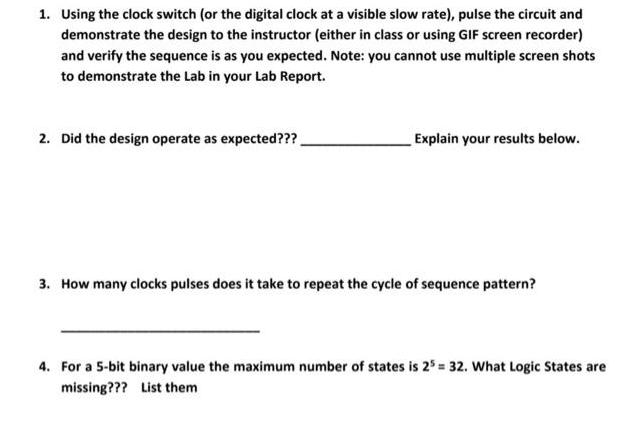
1. Using the clock switch (or the digital clock at a visible slow rate), pulse the circuit and demonstrate the design to the instructor


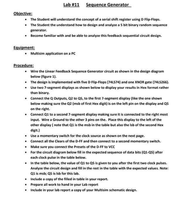
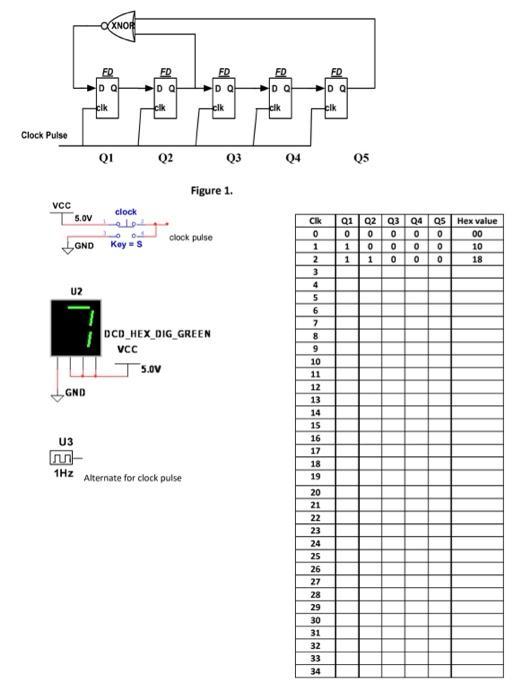
1. Using the clock switch (or the digital clock at a visible slow rate), pulse the circuit and demonstrate the design to the instructor (either in class or using GIF screen recorder) and verify the sequence is as you expected. Note: you cannot use multiple screen shots to demonstrate the Lab in your Lab Report. 2. Did the design operate as expected??? Explain your results below. 3. How many clocks pulses does it take to repeat the cycle of sequence pattern? 4. For a 5-bit binary value the maximum number of states is 25= 32. What Logic States are missing??? List them Equipment: Objective: The Student will understand the concept of a serial shift register using D Flip-Flops. The Student the understand how to design and analyze a 5 bit binary random sequence generator. Become familiar with and be able to analyze this feedback sequential circuit design. Lab # 11 Multisim application on a PC Sequence Generator Procedure: Wire the Linear Feedback Sequence Generator circuit as shown in the design diagram below (figure 1). The design is implemented with five D Flip-Flops (74LS74) and one XNOR gate (74LS266). Use two 7-segment displays as shown below to display your results in Hex format rather than binary. Connect the Q Outputs, Q2 to Q5, to the first 7-segment display (like the one shown below making sure the Q2 (msb of first Hex digit) is on the left pin on the display and Q5 on the right. Connect Q1 to a second 7-segment display making sure it is connected to the right most input. Wire a Ground to the other 3 pins on the. Place this display to the left of the other display (note that Q1 is the msb in the table but also the Isb of the second Hex digit.) Use a momentary switch for the clock source as shown on the next page. Connect all the Clears of the D-FF and then connect to a second momentary switch. Make sure you connect the Presets of the D-FF to VCC . For the circuit diagram below fill in the expected sequence of data bits (Q1-Q5) after each clock pulse in the table below. In the table below, the value of Q1 to Q5 is given to you after the first two clock pulses. Analyze the circuit design and fill in the rest in the table with the expected values. Note: Q1 is msb; Q5 is lsb for this lab. Include a copy of the filled in table in your report. Prepare all work to hand in your Lab report Include in your lab report a copy of your Multisim schematic design. Clock Pulse VCC s.Ov GND U2 U3 GND -OXNOR ED DQ cik Q1 clock 004 Koy = S FD DQ cik Q2 clk clock pulse 1Hz Alternate for clock pulse FD D Q DCD_HEX_DIG GREEN Vcc T5.0V Figure 1. Q3 FD DQ cik Q4 Cik 0 1 2 3 4 5 6 7 8 9 10 11 12 13 14 15 16 17 18 19 20 21 22 23 24 25 26 27 28 29 30 31 32 33 34 FD DQ clk Q5 Q1 Q2 Q3 Q4 Q5 Hex value 0 0 1 0 1 1 GOOG 0 0 0 2000 ... 0 0 00 10 18
Step by Step Solution
★★★★★
3.55 Rating (152 Votes )
There are 3 Steps involved in it
Step: 1
To address the objectives of this lab 1 Using the clock switch or the digital clock at a visible slo...
Get Instant Access to Expert-Tailored Solutions
See step-by-step solutions with expert insights and AI powered tools for academic success
Step: 2

Step: 3

Ace Your Homework with AI
Get the answers you need in no time with our AI-driven, step-by-step assistance
Get Started


