

Answered step by step
Verified Expert Solution
Question
1 Approved Answer
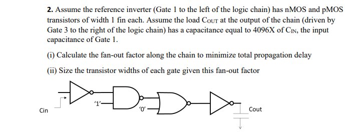
2. Assume the reference inverter (Gate 1 to the left of the logic chain) has nMOS and pMOS transistors of width 1 fin each. Assume
Step by Step Solution
There are 3 Steps involved in it
Step: 1

Get Instant Access to Expert-Tailored Solutions
See step-by-step solutions with expert insights and AI powered tools for academic success
Step: 2

Step: 3
Ace Your Homework with AI
Get the answers you need in no time with our AI-driven, step-by-step assistance
Get Started
Advances In Spatial And Temporal Databases 8th International Symposium Sstd 2003 Santorini Island Greece July 2003 Proceedings Lncs 2750
Authors: Thanasis Hadzilacos ,Yannis Manolopoulos ,John F. Roddick ,Yannis Theodoridis
2003rd Edition
3540405356, 978-3540405351