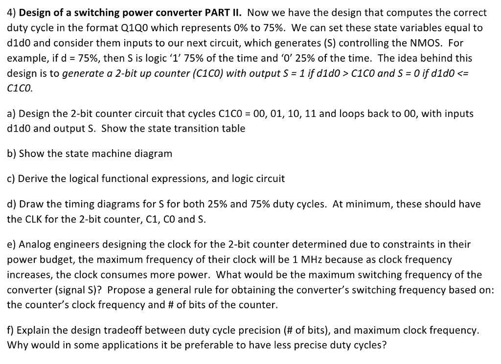
4) Design of a switching power converter PART II. Now we have the design that computes the correct duty cycle in the format Q1Q0 which represents 0% to 75%, we can set these state variables equal to d1d0 and consider them inputs to our next circuit, which generates (S) controlling the NMOS. For example, if d 75%, then S is logic 75% of the time and 25% of the time. The idea behind this design is to generate a 2-bit up counter (CICO) with output S = 1 if d1d0 > CICO and S = 0 if d1d0 = C1CO a) Design the 2-bit counter circuit that cycles C1C0 00, 01, 10, 11 and loops back to 00, with inputs d1d0 and output S. Show the state transition table b) Show the state machine diagram c) Derive the logical functional expressions, and logic circuit d) Draw the timing diagrams for S for both 25% and 75% duty cycles. At minimum, these should have the CLK for the 2-bit counter, C1, CO and S. e) Analog engineers designing the clock for the 2-bit counter determined due to constraints in their power budget, the maximum frequency of their clock wlbe 1 MHz because as clock frequency increases, the clock consumes more power. What would be the maximum switching frequency of the converter (signal S)? Propose a general rule for obtaining the converter's switching frequency based on: the counter's clock frequency and # of bits of the counter f) Explain the design tradeoff between duty cycle precision (# of bits), and maximum clock frequency. Why would in some applications it be preferable to have less precise duty cycles? 4) Design of a switching power converter PART II. Now we have the design that computes the correct duty cycle in the format Q1Q0 which represents 0% to 75%, we can set these state variables equal to d1d0 and consider them inputs to our next circuit, which generates (S) controlling the NMOS. For example, if d 75%, then S is logic 75% of the time and 25% of the time. The idea behind this design is to generate a 2-bit up counter (CICO) with output S = 1 if d1d0 > CICO and S = 0 if d1d0 = C1CO a) Design the 2-bit counter circuit that cycles C1C0 00, 01, 10, 11 and loops back to 00, with inputs d1d0 and output S. Show the state transition table b) Show the state machine diagram c) Derive the logical functional expressions, and logic circuit d) Draw the timing diagrams for S for both 25% and 75% duty cycles. At minimum, these should have the CLK for the 2-bit counter, C1, CO and S. e) Analog engineers designing the clock for the 2-bit counter determined due to constraints in their power budget, the maximum frequency of their clock wlbe 1 MHz because as clock frequency increases, the clock consumes more power. What would be the maximum switching frequency of the converter (signal S)? Propose a general rule for obtaining the converter's switching frequency based on: the counter's clock frequency and # of bits of the counter f) Explain the design tradeoff between duty cycle precision (# of bits), and maximum clock frequency. Why would in some applications it be preferable to have less precise duty cycles


