Answered step by step
Verified Expert Solution
Question
1 Approved Answer
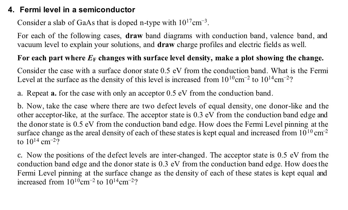
4. Fermi level in a semiconductor Consider a slab of GaAs that is doped n-type with 1017 cm. For each of the following cases,

4. Fermi level in a semiconductor Consider a slab of GaAs that is doped n-type with 1017 cm. For each of the following cases, draw band diagrams with conduction band, valence band, and vacuum level to explain your solutions, and draw charge profiles and electric fields as well. For each part where EF changes with surface level density, make a plot showing the change. Consider the case with a surface donor state 0.5 eV from the conduction band. What is the Fermi Level at the surface as the density of this level is increased from 1010cm 2 to 1014 cm 2? a. Repeat a. for the case with only an acceptor 0.5 eV from the conduction band. b. Now, take the case where there are two defect levels of equal density, one donor-like and the other acceptor-like, at the surface. The acceptor state is 0.3 eV from the conduction band edge and the donor state is 0.5 eV from the conduction band edge. How does the Fermi Level pinning at the surface change as the areal density of each of these states is kept equal and increased from 1010 cm to 1014 cm 2? c. Now the positions of the defect levels are inter-changed. The acceptor state is 0.5 eV from the conduction band edge and the donor state is 0.3 eV from the conduction band edge. How does the Fermi Level pinning at the surface change as the density of each of these states is kept equal and increased from 1010 cm 2 to 1014 cm 2?
Step by Step Solution
There are 3 Steps involved in it
Step: 1

Get Instant Access to Expert-Tailored Solutions
See step-by-step solutions with expert insights and AI powered tools for academic success
Step: 2

Step: 3

Ace Your Homework with AI
Get the answers you need in no time with our AI-driven, step-by-step assistance
Get Started


