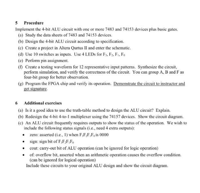
Question: 5 Procedure Implement the 4-bit ALU circuit with one or more 7483 and 74153 devices plus basic gates. (a) Study the data sheets of 7483

5 Procedure Implement the 4-bit ALU circuit with one or more 7483 and 74153 devices plus basic gates. (a) Study the data sheets of 7483 and 74153 devices. (b) Design the 4-bit ALU circuit according to specification. (c) Create a project in Altera Qurtus II and enter the schematic (d) Use 10 switches as inputs. Use 4 LEDs for F3, F2, Fi, Fo (e) Perform pin assignment. (t) Create a testing waveform for 12 representative input patterns. Synthesize the circuit, perform simulation, and verify the correctness of the circuit. You can group A, B and F as four-bit group for better observation. (g) Program the FPGA chip and verify its operation. Demonstrate the circuit to instructor and get signature 6 Additional exercises (a) Is it a good idea to use the truth-table method to design the ALU circuit? Explain. (b) Redesign the 4-bit 4-to-1 multiplexer using the 74157 devices. Show the circuit diagram. (c) An ALU circuit frequently requires outputs to show the status of the operation. We wish to include the following status signals (i.e., need 4 extra outputs) . zero: asserted (i.e., 1) when FF2F,Fo is 0000 sign: sign bit of FF F Fo cout: carry-out bit of ALU operation (can be ignored for logic operation) of: overflow bit, asserted when an arithmctic opcration causes the overflow condition (can be ignored for logical operation) Include these circuits to your original ALU design and show the circuit diagram 5 Procedure Implement the 4-bit ALU circuit with one or more 7483 and 74153 devices plus basic gates. (a) Study the data sheets of 7483 and 74153 devices. (b) Design the 4-bit ALU circuit according to specification. (c) Create a project in Altera Qurtus II and enter the schematic (d) Use 10 switches as inputs. Use 4 LEDs for F3, F2, Fi, Fo (e) Perform pin assignment. (t) Create a testing waveform for 12 representative input patterns. Synthesize the circuit, perform simulation, and verify the correctness of the circuit. You can group A, B and F as four-bit group for better observation. (g) Program the FPGA chip and verify its operation. Demonstrate the circuit to instructor and get signature 6 Additional exercises (a) Is it a good idea to use the truth-table method to design the ALU circuit? Explain. (b) Redesign the 4-bit 4-to-1 multiplexer using the 74157 devices. Show the circuit diagram. (c) An ALU circuit frequently requires outputs to show the status of the operation. We wish to include the following status signals (i.e., need 4 extra outputs) . zero: asserted (i.e., 1) when FF2F,Fo is 0000 sign: sign bit of FF F Fo cout: carry-out bit of ALU operation (can be ignored for logic operation) of: overflow bit, asserted when an arithmctic opcration causes the overflow condition (can be ignored for logical operation) Include these circuits to your original ALU design and show the circuit diagram
Step by Step Solution
There are 3 Steps involved in it

Get step-by-step solutions from verified subject matter experts


