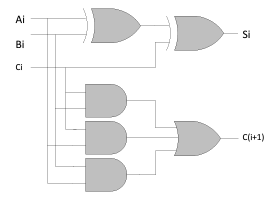
Question
5.1. Show the design is that of a 1- bit full adder by forming the truth tables and equations of the circuit. 5.2 Assume the
5.1. Show the design is that of a 1- bit full adder by forming the truth tables and equations of the circuit.

5.2 Assume the gate delays in the circuit above are 2 ns, 2 ns, and 3 ns for the AND, OR and XO R gates, respectively. When the circuit is used to realize 4- bit ripple carry adders, compute the delay in obtaining C2 , and C3 .
5.3 Compute C6 of the carry- lookahead generator equations.
5.4 Using the delays of gates as given in question 5.2, find the delay for each of the carry equations C1 , C2 , C3 , C4 , C5 , and C6 of a ripple carry adder. Assume the operands are A = A5 A4 A3 A2 A1 A0 and B = B5 B4 B3 B2 B1 B0 . Generalize your answer to compute the delay for Cn. Write your answer in terms of n.
5.6 Show the design of a 2- bit magnitude comparator from 1- bit magnitude comparators.
5.8 An n- bit magnitude comparator can be designed from 1- bit magnitude comparators with enable lines. Show the design of a 5- bit magnitude comparator from 1- bit magnitude comparators with enable lines. Hint the design can be accomplished with five 1- bit comparators and 2 additional gates.
AB CiStep by Step Solution
There are 3 Steps involved in it
Step: 1

Get Instant Access to Expert-Tailored Solutions
See step-by-step solutions with expert insights and AI powered tools for academic success
Step: 2

Step: 3

Ace Your Homework with AI
Get the answers you need in no time with our AI-driven, step-by-step assistance
Get Started


