

Answered step by step
Verified Expert Solution
Question
1 Approved Answer
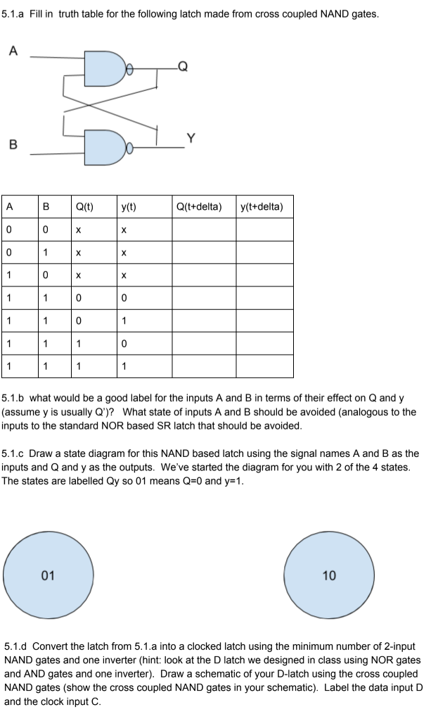
5.1.a Fill in truth table for the following latch made from cross coupled NAND gates. A BQ(t) y(t) Q(t+delta) y(t+delta) 5.1.b what would be a
Step by Step Solution
There are 3 Steps involved in it
Step: 1

Get Instant Access to Expert-Tailored Solutions
See step-by-step solutions with expert insights and AI powered tools for academic success
Step: 2

Step: 3
Ace Your Homework with AI
Get the answers you need in no time with our AI-driven, step-by-step assistance
Get Started
Advances In Spatial Databases 5th International Symposium Ssd 97 Berlin Germany July 15 18 1997 Proceedings Lncs 1262
Authors: Michel Scholl ,Agnes Voisard
1st Edition
3540632387, 978-3540632382