Answered step by step
Verified Expert Solution
Link Copied!

Question

1 Approved Answer

#6. Implement the following SOP (Sum of Products) logic function in all NAND gate form, and draw the resulting circuit schematic: LOGIC DESIGN & SIMPLIFICATION:
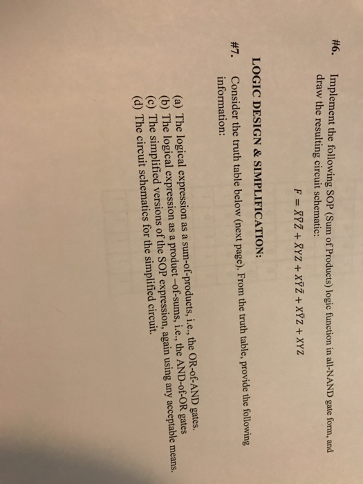
image text in transcribed
#6. Implement the following SOP (Sum of Products) logic function in all NAND gate form, and draw the resulting circuit schematic: LOGIC DESIGN & SIMPLIFICATION: Consider the truth table below (next page). From the truth table, provide the following information: (a) The logical expression as a sum-of-products, i.e., the OR-of-AND gates (b) The logical expression as a product -of-sums, i.e., the AND-of-OR gates (c) The simplified versions of the SOP expression, again using any acceptable means. (d) The circuit schematics for the simplified circuit

Step by Step Solution

There are 3 Steps involved in it

Step: 1

blur-text-image

Get Instant Access to Expert-Tailored Solutions

See step-by-step solutions with expert insights and AI powered tools for academic success

Step: 2

blur-text-image_2

Step: 3

blur-text-image_3

Ace Your Homework with AI

Get the answers you need in no time with our AI-driven, step-by-step assistance

Get Started

Recommended Textbook for

Optimizing Data Collection In Warzones

Authors: Aaget Aamber

1st Edition

B0CQRRFP5F, 979-8869065902

More Books

Students also viewed these Databases questions