

Answered step by step
Verified Expert Solution
Question
1 Approved Answer
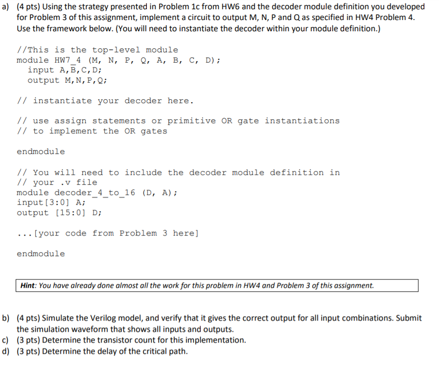
a) (4 pts) Using the strategy presented in Problem 1c from HW6 and the decoder module definition you developed for Problem 3 of this assignment,
Step by Step Solution
There are 3 Steps involved in it
Step: 1

Get Instant Access to Expert-Tailored Solutions
See step-by-step solutions with expert insights and AI powered tools for academic success
Step: 2

Step: 3
Ace Your Homework with AI
Get the answers you need in no time with our AI-driven, step-by-step assistance
Get Started
Database Modeling And Design
Authors: Toby J. Teorey, Sam S. Lightstone, Tom Nadeau, H.V. Jagadish
5th Edition
0123820200, 978-0123820204