

Answered step by step
Verified Expert Solution
Question
1 Approved Answer
A common-emitter amplifier is shown in Fig. 4. In this circuit, the input signal is a 1 kHz sinusoidal wave with an amplitude of
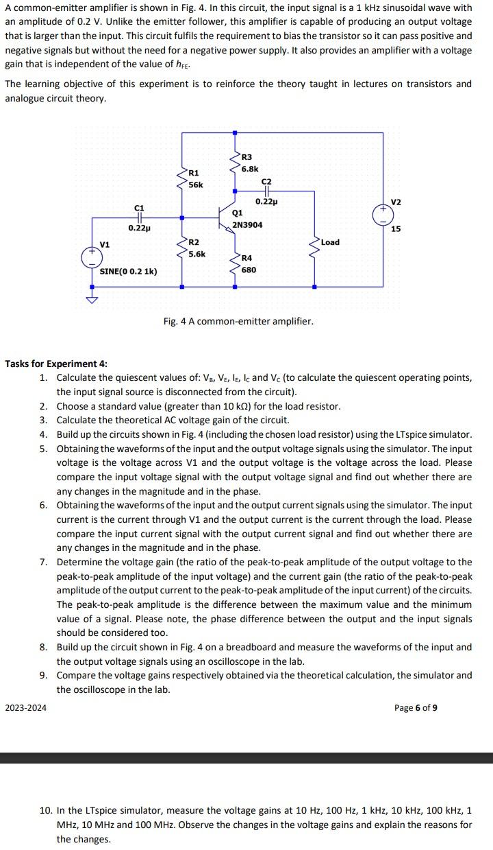
A common-emitter amplifier is shown in Fig. 4. In this circuit, the input signal is a 1 kHz sinusoidal wave with an amplitude of 0.2 V. Unlike the emitter follower, this amplifier is capable of producing an output voltage that is larger than the input. This circuit fulfils the requirement to bias the transistor so it can pass positive and negative signals but without the need for a negative power supply. It also provides an amplifier with a voltage gain that is independent of the value of hFE. The learning objective of this experiment is to reinforce the theory taught in lectures on transistors and analogue circuit theory. V1 C1 0.22 SINE(0 0.2 1k) 2023-2024 R1 56k R2 5.6k R3 6.8k C2 0.22 Q1 2N3904 R4 680 Fig. 4 A common-emitter amplifier. Load V2 15 Tasks for Experiment 4: 1. Calculate the quiescent values of: VB, VE, IE, IC and Vc (to calculate the quiescent operating points, the input signal source is disconnected from the circuit). 2. Choose a standard value (greater than 10 k) for the load resistor. 3. Calculate the theoretical AC voltage gain of the circuit. 4. Build up the circuits shown in Fig. 4 (including the chosen load resistor) using the LTspice simulator. 5. Obtaining the waveforms of the input and the output voltage signals using the simulator. The input voltage is the voltage across V1 and the output voltage is the voltage across the load. Please compare the input voltage signal with the output voltage signal and find out whether there are any changes in the magnitude and in the phase. 6. Obtaining the waveforms of the input and the output current signals using the simulator. The input current is the current through V1 and the output current is the current through the load. Please compare the input current signal with the output current signal and find out whether there are any changes in the magnitude and in the phase. 7. Determine the voltage gain (the ratio of the peak-to-peak amplitude of the output voltage to the peak-to-peak amplitude of the input voltage) and the current gain (the ratio of the peak-to-peak amplitude of the output current to the peak-to-peak amplitude of the input current) of the circuits. The peak-to-peak amplitude is the difference between the maximum value and the minimum value of a signal. Please note, the phase difference between the output and the input signals should be considered too. 8. Build up the circuit shown in Fig. 4 on a breadboard and measure the waveforms of the input and the output voltage signals using an oscilloscope in the lab. 9. Compare the voltage gains respectively obtained via the theoretical calculation, the simulator and the oscilloscope in the lab. Page 6 of 9 10. In the LTspice simulator, measure the voltage gains at 10 Hz, 100 Hz, 1 kHz, 10 kHz, 100 kHz, 1 MHz, 10 MHz and 100 MHz. Observe the changes in the voltage gains and explain the reasons for the changes.
Step by Step Solution
★★★★★
3.52 Rating (159 Votes )
There are 3 Steps involved in it
Step: 1
Task 1 Calculate the quiescent values of the circuit components To calculate the quiescent values of the circuit components we need to disconnect the ...
Get Instant Access to Expert-Tailored Solutions
See step-by-step solutions with expert insights and AI powered tools for academic success
Step: 2

Step: 3
Ace Your Homework with AI
Get the answers you need in no time with our AI-driven, step-by-step assistance
Get Started
Analysis and Design of Analog Integrated Circuits
Authors: Paul R. Gray, Paul J. Hurst Stephen H. Lewis, Robert G. Meyer
5th edition
1111827052, 1285401107, 9781285401102 , 978-0470245996