

Answered step by step
Verified Expert Solution
Question
1 Approved Answer
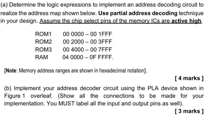
(a) Determine the logic expressions to implement an address decoding circuit to realize the address map shown below. Use partial address decoding technique in your
Step by Step Solution
There are 3 Steps involved in it
Step: 1

Get Instant Access to Expert-Tailored Solutions
See step-by-step solutions with expert insights and AI powered tools for academic success
Step: 2

Step: 3
Ace Your Homework with AI
Get the answers you need in no time with our AI-driven, step-by-step assistance
Get Started
Online Systems For Physicians And Medical Professionals How To Use And Access Databases
Authors: Harley Bjelland
1st Edition
1878487442, 9781878487445