Answered step by step
Verified Expert Solution
Question
1 Approved Answer
a. Sketch a transistor layout, and Euler path, and a stick diagram for each of the following Boolean functions. You may assume that you have
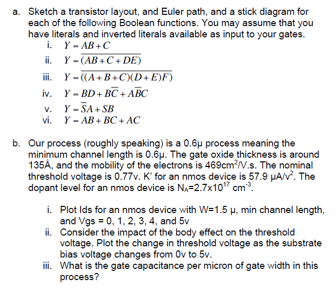
a. Sketch a transistor layout, and Euler path, and a stick diagram for each of the following Boolean functions. You may assume that you have literals and inverted literals available as input to your gates. i. Y=AB + C ii. Y=(AB + C + DE) ii Y - ((A+B+C)(D+E)F) iv. Y- BD+ BC+ABC vi. Y- AB+BC +AC Our process (roughly speaking) is a 0.6 process meaning the minimum channel length is 0.6. The gate oxidethickness is around 135A, andio mobility of tho ekotrens is 469cr/.s. . I nominal threshold voltage is 0.77v. K, for an nmos device is 57.9 A/ The dopant level for an nmos device is NA-2.7x1017 cm3 b. i. Plot Ids for an nmos device with W= 1.5 , min channel length, and Vgs Consider the) impact voltage. Plot the change in threshold voltage as the substrate bias voltage changes from 0v to 5v. 0, 1, 2, 3, 4, and 5v ii. tho body cif)()n tho thiesheld ii. What is the gate capacitance per micron of gate width in this process
Step by Step Solution
There are 3 Steps involved in it
Step: 1
Get Instant Access to Expert-Tailored Solutions
See step-by-step solutions with expert insights and AI powered tools for academic success
Step: 2
Step: 3
Ace Your Homework with AI
Get the answers you need in no time with our AI-driven, step-by-step assistance
Get Started