Answered step by step
Verified Expert Solution
Question
1 Approved Answer
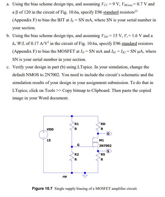
a. Using the bias scheme design tips, and assuming Vcc=9V, VBE(on) 0.7 V and a 3 of 120 in the circuit of Fig. 10.6a,

a. Using the bias scheme design tips, and assuming Vcc=9V, VBE(on) 0.7 V and a 3 of 120 in the circuit of Fig. 10.6a, specify E96 standard resistors 23 (Appendix F) to bias the BJT at lg = SN mA, where SN is your serial number in your section. b. Using the bias scheme design tips, and assuming VDD = 15 V, V,= 1.6 V and a ka W/L of 0.17 A/V in the circuit of Fig. 10.6a, specify E96 standard resistors (Appendix F) to bias the MOSFET at ID - SN mA and IR = IR2 = SN A, where SN is your serial number in your section. = c. Verify your design in part (b) using LTspice. In your simulation, change the default NMOS to 2N7002. You need to include the circuit's schematic and the simulation results of your design in your assignment submission. To do that in LTspice, click on Tools >> Copy bitmap to Clipboard. Then paste the copied image in your Word document. VDD 15 .op R1 R G R2 R RD R M1 2N7002 RS R Figure 10.7 Single supply biasing of a MOSFET amplifier circuit.
Step by Step Solution
★★★★★
3.41 Rating (167 Votes )
There are 3 Steps involved in it
Step: 1
a Using the given values of Vcc9V VBEon 07 V and a of 120 if my serial number is 21 the...
Get Instant Access to Expert-Tailored Solutions
See step-by-step solutions with expert insights and AI powered tools for academic success
Step: 2

Step: 3

Ace Your Homework with AI
Get the answers you need in no time with our AI-driven, step-by-step assistance
Get Started


