

Question: Assignment 12: 16-bit Integrator Objective The objective of this assignment is to introduce the Controllers and Datapath concept in Digital Design You will be designing
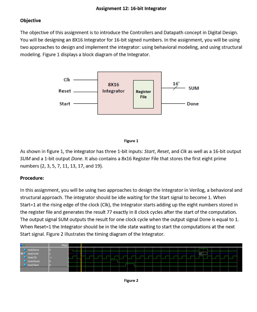
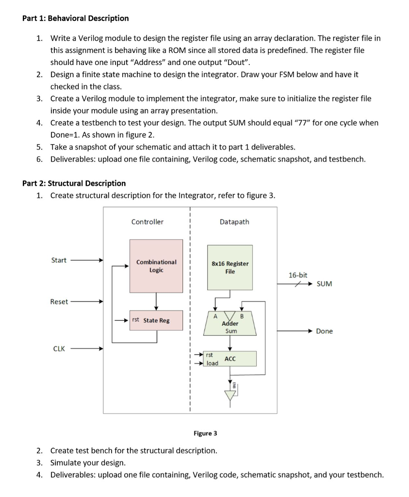
Assignment 12: 16-bit Integrator Objective The objective of this assignment is to introduce the Controllers and Datapath concept in Digital Design You will be designing an 8X16 Integrator for 16-bit signed numbers. In the assignment, you will be using two approaches to design and implement the integrator: using behavioral modeling, and using structural modeling. Figure 1 displays a block diagram of the Integrator CIk 8X16 16 SUM Reset Integrator Register File Start Done Figure 1 As shown in figure 1, the integrator has three 1-bit inputs: Start, Reset, and Clk as well as a 16-bit output SUM and a 1-bit output Done. It also contains a 8x16 Register File that stores the first eight prime numbers (2, 3, 5,7, 11,13, 17, and 19) Procedure: In this assignment, you will be using two approaches to design the Integrator in Verilog, a behavioral and structural approach. The integrator should be idle waiting for the Start signal to become 1. When Start 1 at the rising edge of the clock (Clk), the Integrator starts adding up the eight numbers stored in the register file and generates the result 77 exactly in 8 clock cycles after the start of the computation The output signal SUM outputs the result for one clock cycle when the output signal Done is equal to 1 When Reset-1 the Integrator should be in the Idle state waiting to start the computations at the next Start signal. Figure 2 illustrates the timing diagram of the Integrator Msgs /test/Done /test/Clk Figure 2 Part 1: Behavioral Description 1. Write a Verilog module to design the register file using an array declaration. The register file in this assignment is behaving like a ROM since all stored data is predefined. The register file should have one input "Address" and one output "Dout" Design a finite state machine to design the integrator. Draw your FSM below and have it checked in the class Create a Verilog module to implement the integrator, make sure to initialize the register file inside your module using an array presentation 2. 3. 4. Create a testbench to test your design. The output SUM should equal "77" for one cycle whern 5. 6. Done-1. As shown in figure 2 Take a snapshot of your schematic and attach it to part 1 deliverables Deliverables: upload one file containing, Verilog code, schematic snapshot, and testbench Part 2: Structural Description 1. Create structural description for the Integrator, refer to figure 3 Controller Datapath Start CombinationalI 8x16 Register File Logic 16-bit SUM Reset rst State Reg Adder Sum Done CLK rst ACC oad Figure 3 2. 3. 4. Create test bench for the structural description. Simulate your design Deliverables: upload one file containing, Verilog code, schematic snapshot, and your testbench Assignment 12: 16-bit Integrator Objective The objective of this assignment is to introduce the Controllers and Datapath concept in Digital Design You will be designing an 8X16 Integrator for 16-bit signed numbers. In the assignment, you will be using two approaches to design and implement the integrator: using behavioral modeling, and using structural modeling. Figure 1 displays a block diagram of the Integrator CIk 8X16 16 SUM Reset Integrator Register File Start Done Figure 1 As shown in figure 1, the integrator has three 1-bit inputs: Start, Reset, and Clk as well as a 16-bit output SUM and a 1-bit output Done. It also contains a 8x16 Register File that stores the first eight prime numbers (2, 3, 5,7, 11,13, 17, and 19) Procedure: In this assignment, you will be using two approaches to design the Integrator in Verilog, a behavioral and structural approach. The integrator should be idle waiting for the Start signal to become 1. When Start 1 at the rising edge of the clock (Clk), the Integrator starts adding up the eight numbers stored in the register file and generates the result 77 exactly in 8 clock cycles after the start of the computation The output signal SUM outputs the result for one clock cycle when the output signal Done is equal to 1 When Reset-1 the Integrator should be in the Idle state waiting to start the computations at the next Start signal. Figure 2 illustrates the timing diagram of the Integrator Msgs /test/Done /test/Clk Figure 2 Part 1: Behavioral Description 1. Write a Verilog module to design the register file using an array declaration. The register file in this assignment is behaving like a ROM since all stored data is predefined. The register file should have one input "Address" and one output "Dout" Design a finite state machine to design the integrator. Draw your FSM below and have it checked in the class Create a Verilog module to implement the integrator, make sure to initialize the register file inside your module using an array presentation 2. 3. 4. Create a testbench to test your design. The output SUM should equal "77" for one cycle whern 5. 6. Done-1. As shown in figure 2 Take a snapshot of your schematic and attach it to part 1 deliverables Deliverables: upload one file containing, Verilog code, schematic snapshot, and testbench Part 2: Structural Description 1. Create structural description for the Integrator, refer to figure 3 Controller Datapath Start CombinationalI 8x16 Register File Logic 16-bit SUM Reset rst State Reg Adder Sum Done CLK rst ACC oad Figure 3 2. 3. 4. Create test bench for the structural description. Simulate your design Deliverables: upload one file containing, Verilog code, schematic snapshot, and your testbench
Step by Step Solution
There are 3 Steps involved in it

Get step-by-step solutions from verified subject matter experts