Question
Assume logic gate delays are given in terms of a time delay term (t, t is in nano-seconds). Assume as well, logic gate delays are:
Assume logic gate delays are given in terms of a time delay term (t, t is in nano-seconds). Assume as well, logic gate delays are: 1 t for the logic gates NOT, NAND, and NOR, 2 t for the logic gates AND and OR; and 3 t for the logic gates XOR and XNOR. The delays given are independent of the number of inputs to each logic gate (this is normally not the case). Compute the delays, in terms of t, for the carry outs C1, C2, C3, , Cn (general n) and sums S0, S1, S2, , Sn, for the two designs of the n-bit full adder:
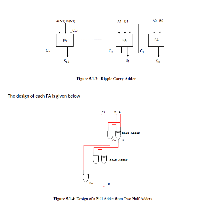
(a) the ripple-carry as given in Figure 5.1.2 (assume stage 0 of the figure is a full adder). All stages are designed similar to figure 5.1.4.
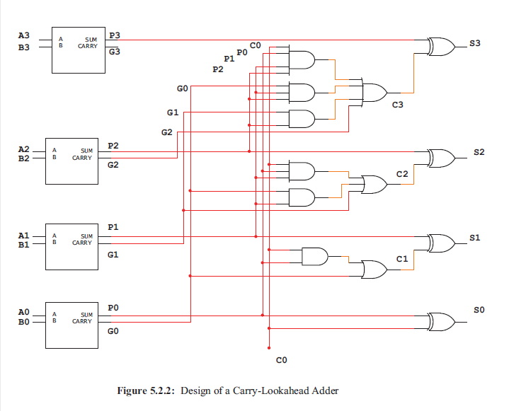
(b) The carry-lookahead adder as given in Figure 5.2.2.


A(n-1) B (n-1) A1 B1 AD BO FA FA FA CI SI So Figure 5.1.2: Ripple Carry Adder The design of each FA is given below Ci B A Half Adder Half Adder Co Figure 5.1.4: Design of a Full Adder from Two Half Adders B3 P3 SUM B CARRY CO S3 G3 PO P1 P2 GO C3 G1 G2 P2 A2 B2 S2 B CARRY G2 C2 P1 A1 B1 SUM CARRY S1 B G1 C1 PO SO A0 BO SUM CARRY B GO Co Figure 5.2.2: Design of a Carry-Lookahead Adder A(n-1) B (n-1) A1 B1 AD BO FA FA FA CI SI So Figure 5.1.2: Ripple Carry Adder The design of each FA is given below Ci B A Half Adder Half Adder Co Figure 5.1.4: Design of a Full Adder from Two Half Adders B3 P3 SUM B CARRY CO S3 G3 PO P1 P2 GO C3 G1 G2 P2 A2 B2 S2 B CARRY G2 C2 P1 A1 B1 SUM CARRY S1 B G1 C1 PO SO A0 BO SUM CARRY B GO Co Figure 5.2.2: Design of a Carry-Lookahead Adder
Step by Step Solution
There are 3 Steps involved in it
Step: 1

Get Instant Access to Expert-Tailored Solutions
See step-by-step solutions with expert insights and AI powered tools for academic success
Step: 2

Step: 3

Ace Your Homework with AI
Get the answers you need in no time with our AI-driven, step-by-step assistance
Get Started


