

Answered step by step
Verified Expert Solution
Question
1 Approved Answer
Bus Memory Bus Address Memory unit 4096 X 16 Address Write Read AR LD INR CLR TAR PC I LD INR CLR Write Read AR
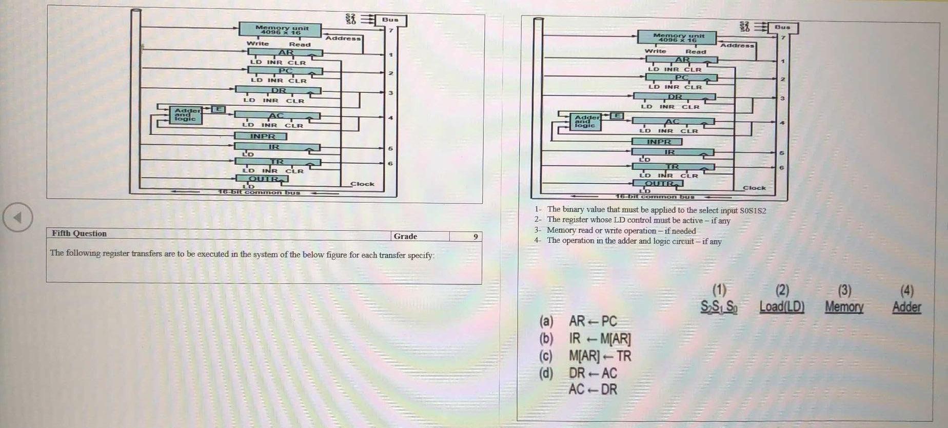
Bus Memory Bus Address Memory unit 4096 X 16 Address Write Read AR LD INR CLR TAR PC I LD INR CLR Write Read AR LD INR CLR PC LD INR CLR DR LD INR CLR DR Adder logic E Adder and logic LD INR CLR IE AC LD INR CLR INPR IR Lo TR LD INR CLR OIR LD 16 bit common bus AC LD INR CLR INPR IR LD IR LO NR CLR 6 Clock Clock 16-bit common bus 1- The binary value that must be applied to the select input SOS1S2 2- The register whose LD control must be active - if any 3- Memory read or write operation - if needed 4 The operation in the adder and logic circuit - if any Fifth Question Grade The following register transfers are to be executed in the system of the below figure for each transfer specify: SS, SO (2) Load(LD) (3) Memory Adder (a) AR - PC (b) IR M[AR] () M[AR]- TR (d) DRAC AC - DR
Step by Step Solution
There are 3 Steps involved in it
Step: 1

Get Instant Access to Expert-Tailored Solutions
See step-by-step solutions with expert insights and AI powered tools for academic success
Step: 2

Step: 3
Ace Your Homework with AI
Get the answers you need in no time with our AI-driven, step-by-step assistance
Get Started
Applications Of Databases First International Conference Adb 94 Vadstena Sweden June 21 23 1994 Proceedings Lncs 819
Authors: Witold Litwin ,Tore Risch
1st Edition
3540581839, 978-3540581833