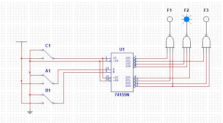
Answered step by step
Verified Expert Solution
Link Copied!

Question

1 Approved Answer

Can someone please explain why the output in this multiim simulation is not matching my truth table? I know my truth table is correct as

Can someone please explain why the output in this multiim simulation is not matching my truth table? I know my truth table is correct as I have verified through multiple comparisons of others. I am using the minterms from my truth table to wire the output to nand gates as instructed by my handout, however it gives me a completely different output then what I have on my truth table. Please help. Please understand, I am looking for a proper explanation, not just an answer. If writing by hand, please write legibly, also if you are answering my question with a multisim simulation, please explain why yours works and matches my truth table, and mine does not.image text in transcribedimage text in transcribedimage text in transcribedimage text in transcribed

CIRCUIT 3 INPUT A B C A B' AC AB A'B A'B'C' A'B'C AB'C' 0 0 1 1 1 0 1 0 1 0 0 0 0 1 1 0 0 0 0 1 0 0 0 0 1 1 1 0 0 1 0 1 1 0 1 0 0 0 0 OUTPUT F1 F2 F3 AC+A'B'C' A'B+AB'C' AB+A'B'C 0 1 0 0 0 0 1 0 1 0 0 0 1 0 1 0 1 0 0 1 0 0 0 0 0 1 0 1 0 1 0 0 0 1 0 1 1 1 0 0 0 0 0 1 0 1 0 0 1 0 0 0 0 0 0 0 1 0 0 1 1 0 1 1 1 0 1 0 1 0 0 F1 F2 F3 C1 U1 IYO 1C 1G 172 ET A1 B 15 19) 270. -2C 2G B. .243 B1 74155N . HI . 3. A combinational circuit has 3 inputs: x, y and z, and 3 outputs: F1, F2 and F3. The simplified Boolean functions for the circuit are F1 = AC + A'B'C' F2 = A'B + AB'C' F3 = AB + A'B'C Implement and test the combinational circuit, using a 74155 decoder IC and some external logic gates. The block diagram of the decoder and its truth table are shown below. The 74155 can be connected as a dual 2x4 decoder or as a single 3x8 decoder. When a 3x8 decoder is desired, inputs C1 and C2, as well as G1 and G2, must be connected together, as shown in the block diagram. G is the enable input and must be equal to 0 for proper operation. The 8 outputs are labeled with symbols given in the data book. The 74155 uses NAND gates, with the result that the selected output goes to o while all other outputs remain at 1. a. Verify the function table of the decoder 74155. b. Derive the truth-table for F1, F2 and F3 c. Draw the logic diagram for implementing F1, F2 and F3 using a 3x8 decoder and some external logic gates. d. Use 74155, 7427 and 7404 to verify your implementation 16 Voc 1 C1 15 C C2 3 B B 9 2Y0 10 241 11 2Y2 12 2Y3 7 1Y0 6 1Y1 5 TY2 4 1Y3 13 74155 2 G1 14 G2 GND 8 Truth table Outputs 2Y3 IYO G 2Y0 271 272 171 172 1Y3 1 1 1 1 0 0 0 0 0 0 0 0 Inputs C B X X 0 0 0 0 0 1 0 1 1 0 1 0 1 1 1 1 X 0 1 0 1 0 1 0 1 1 0 1 1 1 1 1 1 1 1 1 0 1 1 1 1 1 1 1 1 1 0 1 1 1 1 1 1 1 1 1 0 1 1 1 1 1 1 1 0 1 1 1 1 1 1 1 1 1 0 1 1 1 1 1 1 1 1 1 0 1 1 1 1 0 Fig. 11-7 IC Type 74155 Connected as a 3 x 8 Decoder

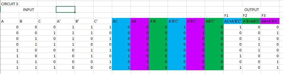
Step by Step Solution

There are 3 Steps involved in it

Step: 1

blur-text-image

Get Instant Access to Expert-Tailored Solutions

See step-by-step solutions with expert insights and AI powered tools for academic success

Step: 2

blur-text-image

Step: 3

blur-text-image

Ace Your Homework with AI

Get the answers you need in no time with our AI-driven, step-by-step assistance

Get Started

Recommended Textbook for

Database Internals A Deep Dive Into How Distributed Data Systems Work

Authors: Alex Petrov

1st Edition

1492040347, 978-1492040347

More Books

Students also viewed these Databases questions

Question

What is the basis for Security Concerns in Cloud Computing?

Answered: 1 week ago

Question

Describe the three main Cloud Computing Environments.

Answered: 1 week ago