Answered step by step
Verified Expert Solution
Question
1 Approved Answer
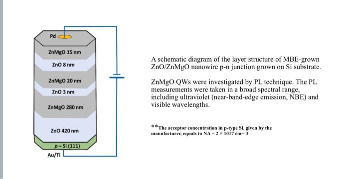
can you explain this photo , about p-n junction for inorganic chemistry ZnMgO 15 nm ZnO 8 nm ZnMgo 20 nm ZnO 3 nm ZnMgO
can you explain this photo , about p-n junction for inorganic chemistry 
ZnMgO 15 nm ZnO 8 nm ZnMgo 20 nm ZnO 3 nm ZnMgO 280 nm A schematic diagram of the layer structure of MBE-grown Zno/ZnMgO nanowire p-n junction grown on Si substrate. ZnMgO QWs were investigated by PL technique. The PL measurements were taken in a broad spectral range, including ultraviolet (near-band-edge emission, NBE) and visible wavelengths. ZnO 420 nm **The acceptor concentration in p-type Si, given by the manufacturer, equals to NA=2 x 1017 cm-3 p-Si (111) Au/Ti 
Step by Step Solution
There are 3 Steps involved in it
Step: 1

Get Instant Access to Expert-Tailored Solutions
See step-by-step solutions with expert insights and AI powered tools for academic success
Step: 2

Step: 3

Ace Your Homework with AI
Get the answers you need in no time with our AI-driven, step-by-step assistance
Get Started


