Question: Can you simulate this lab plzz 1. Semiconductor Diodes - Brief Introduction and Terminology A semiconductor diode is a two-terminal device formed by the junction
Can you simulate this lab plzz


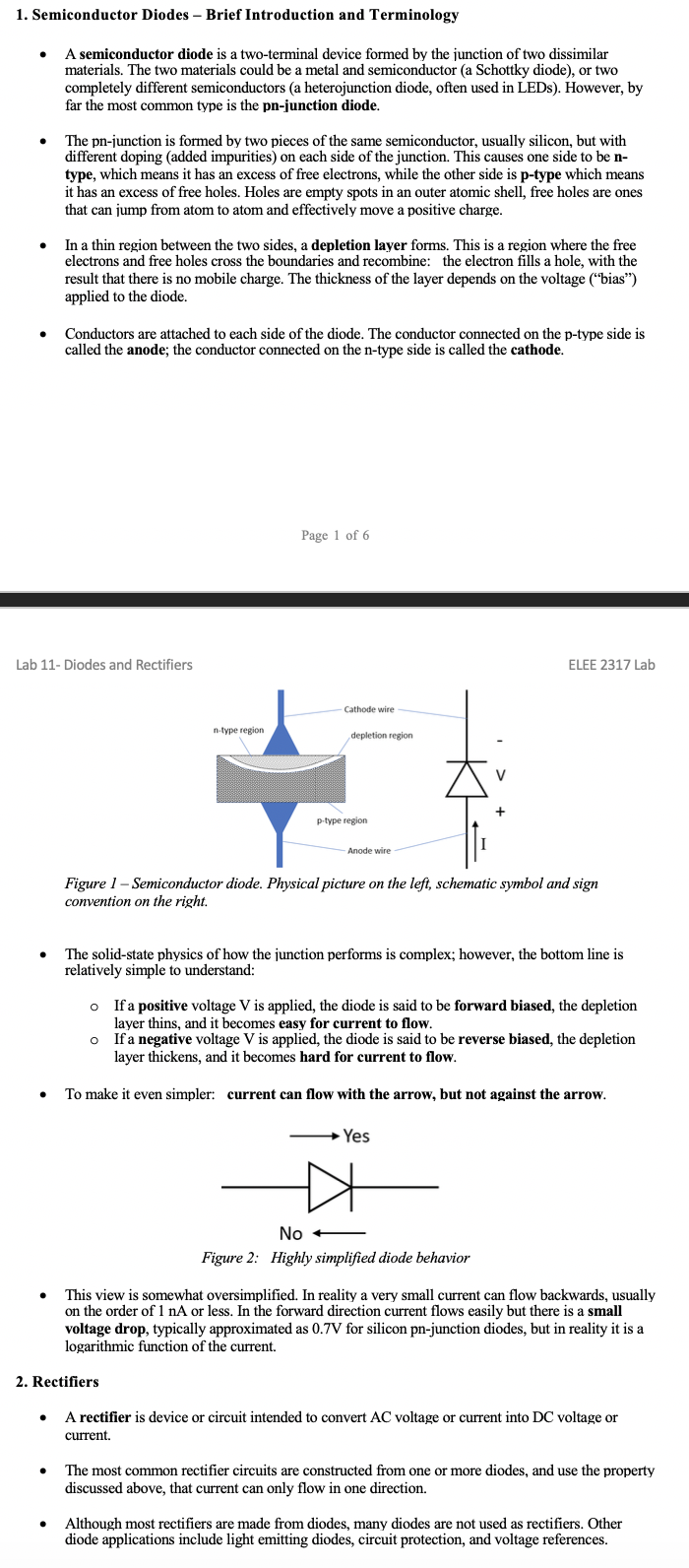
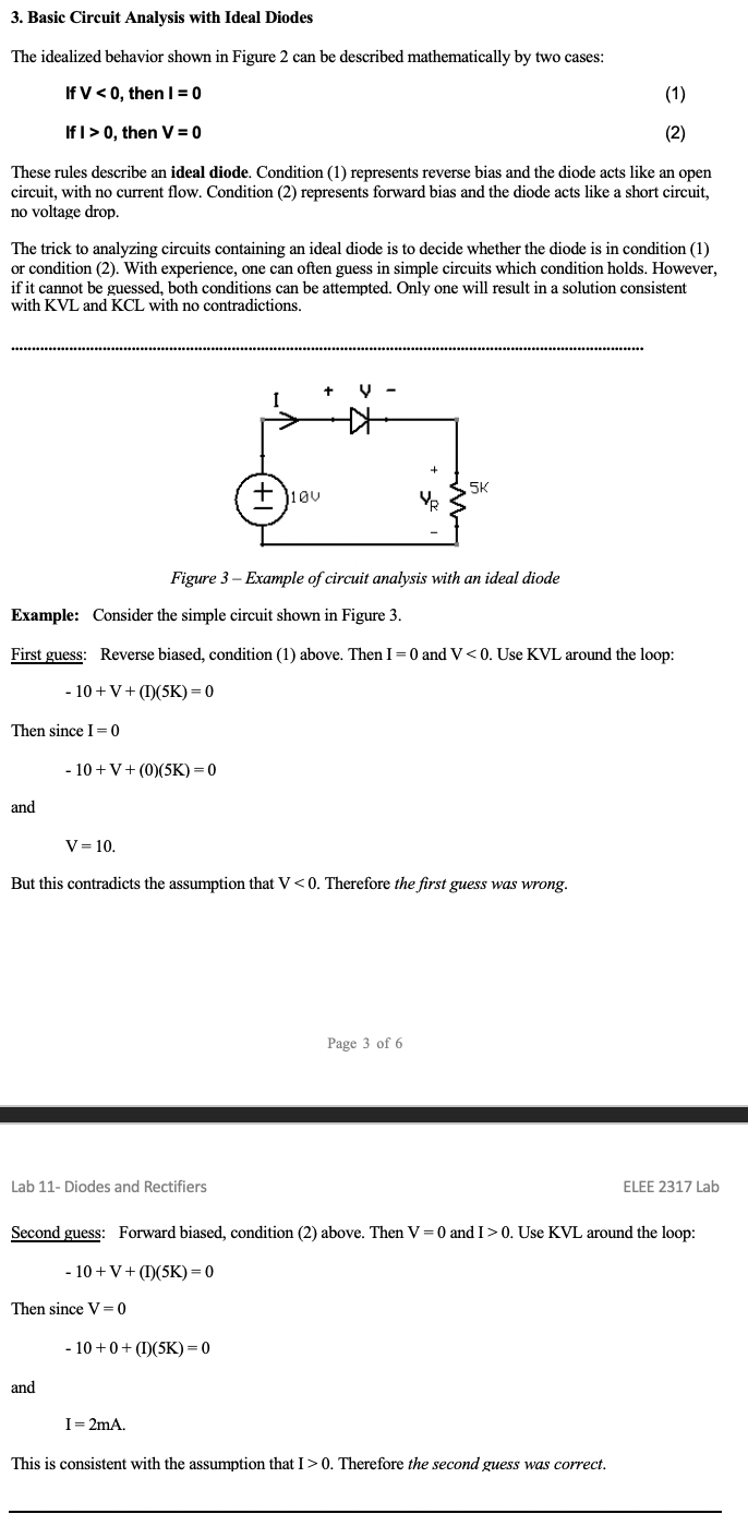
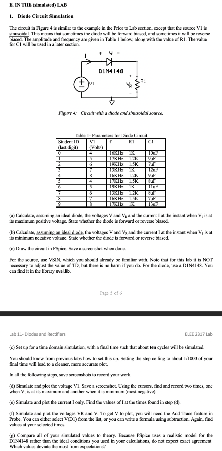
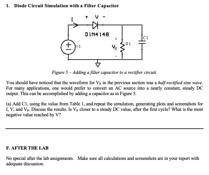
1. Semiconductor Diodes - Brief Introduction and Terminology A semiconductor diode is a two-terminal device formed by the junction of two dissimilar materials. The two materials could be a metal and semiconductor (a Schottky diode), or two completely different semiconductors (a heterojunction diode, often used in LEDs). However, by far the most common type is the pn-junction diode. The pn-junction is formed by two pieces of the same semiconductor, usually silicon, but with different doping (added impurities) on each side of the junction. This causes one side to be n- type, which means it has an excess of free electrons, while the other side is p-type which means it has an excess of free holes. Holes are empty spots in an outer atomic shell, free holes are ones that can jump from atom to atom and effectively move a positive charge. In a thin region between the two sides, a depletion layer forms. This is a region where the free electrons and free holes cross the boundaries and recombine: the electron fills a hole, with the result that there is no mobile charge. The thickness of the layer depends on the voltage ("bias") applied to the diode. Conductors are attached to each side of the diode. The conductor connected on the p-type side is called the anode; the conductor connected on the n-type side is called the cathode. Page 1 of 6 Lab 11- Diodes and Rectifiers ELEE 2317 Lab Cathode wire n-type region depletion region I > + p-type region - Anode wire Figure 1 - Semiconductor diode. Physical picture on the left, schematic symbol and sign convention on the right. The solid-state physics of how the junction performs is complex; however, the bottom line is relatively simple to understand: o o If a positive voltage V is applied, the diode is said to be forward biased, the depletion layer thins, and it becomes easy for current to flow. If a negative voltage V is applied, the diode is said to be reverse biased, the depletion layer thickens, and it becomes hard for current to flow. To make it even simpler: current can flow with the arrow, but not against the arrow. Yes No Figure 2: Highly simplified diode behavior This view is somewhat oversimplified. In reality a very small current can flow backwards, usually on the order of 1 nA or less. In the forward direction current flows easily but there is a small voltage drop, typically approximated as 0.7V for silicon pn-junction diodes, but in reality it is a logarithmic function of the current. 2. Rectifiers A rectifier is device or circuit intended to convert AC voltage or current into DC voltage or current. The most common rectifier circuits are constructed from one or more diodes, and use the property discussed above, that current can only flow in one direction. Although most rectifiers are made from diodes, many diodes are not used as rectifiers. Other diode applications include light emitting diodes, circuit protection, and voltage references. 3. Basic Circuit Analysis with Ideal Diodes The idealized behavior shown in Figure 2 can be described mathematically by two cases: If V 0, then V = 0 These rules describe an ideal diode. Condition (1) represents reverse bias and the diode acts like an open circuit, with no current flow. Condition (2) represents forward bias and the diode acts like a short circuit, no voltage drop. The trick to analyzing circuits containing an ideal diode is to decide whether the diode is in condition (1) or condition (2). With experience, one can often guess in simple circuits which condition holds. However, if it cannot be guessed, both conditions can be attempted. Only one will result in a solution consistent with KVL and KCL with no contradictions. + 10v % 35K Figure 3 - Example of circuit analysis with an ideal diode Example: Consider the simple circuit shown in Figure 3. First guess: Reverse biased, condition (1) above. Then I = 0 and V0. Use KVL around the loop: - 10+V+ (1)(5K)=0 Then since V=0 - 10+0+ (1)(5K)=0 and I= 2mA. This is consistent with the assumption that I > 0. Therefore the second guess was correct. E. IN THE (simulated) LAB 1. Diode Circuit Simulation The circuit in Figure 4 is similar to the example in the Prior to Lab section, except that the source V1 is sinusoidal. This means that sometimes the diode will be forward biased, and sometimes it will be reverse biased. The amplitude and frequency are given in Table 1 below, along with the value of R1. The value for C1 will be used in a later section. + V - D1N4148 - Figure 4: Circuit with a diode and sinusoidal source. C1 Table 1- Parameters for Diode Circuit Student ID vi (last digit) (Volts) 16KHZ IK 10uF 17KHZ 1.2K 9uF 19KHz 1.5K 7uF 13KHZIK 12uF 16KHz 1.2K Out 17KHZ 1.5K Suf 19KHZIK 11uF 6 13KHZ 1.2K 8uF 8 7 16KHz 1.5K 9 8 | 17KHZIK 13uF ZUF (a) Calculate, assuming an ideal diode, the voltages V and VR and the current I at the instant when V, is at its maximum positive voltage. State whether the diode is forward or reverse biased. (b) Calculate, assuming an ideal diode, the voltages V and VR and the current I at the instant when Vi is at its minimum negative voltage. State whether the diode is forward or reverse biased. (c) Draw the circuit in PSpice. Save a screenshot when done. For the source, use VSIN, which you should already be familiar with. Note that for this lab it is NOT necessary to adjust the value of TD, but there is no harm if you do. For the diode, use a DIN4148. You can find it in the library eval.lib. Page 5 of 6 Lab 11- Diodes and Rectifiers ELEE 2317 Lab (c) Set up for a time domain simulation, with a final time such that about ten cycles will be simulated. You should know from previous labs how to set this up. Setting the step ceiling to about 1/1000 of your final time will lead to a cleaner, more accurate plot. In all the following steps, save screenshots to record your work. (d) Simulate and plot the voltage V1. Save a screenshot. Using the cursors, find and record two times, one when V, is at its maximum and another when it is minimum (most negative). (e) Simulate and plot the current I only. Find the values of I at the times found in step (d). (f) Simulate and plot the voltages VR and V. To get V to plot, you will need the Add Trace feature in Probe. You can either select V(D1) from the list, or you can write a formula using subtraction. Again, find values at your selected times. (g) Compare all of your simulated values to theory. Because PSpice uses a realistic model for the D1N4148 rather than the ideal conditions you used in your calculations, do not expect exact agreement. Which values deviate the most from expectations? 1. Diode Circuit Simulation with a Filter Capacitor D1N4148 {R1 Figure 5 - Adding a filter capacitor to a rectifier circuit. You should have noticed that the waveform for VR in the previous section was a half-rectified sine wave. For many applications, one would prefer to convert an AC source into a nearly constant, steady DC output. This can be accomplished by adding a capacitor as in Figure 5. (a) Add C1, using the value from Table 1, and repeat the simulation, generating plots and screenshots for I, V, and V. Discuss the results. Is VR closer to a steady DC value, after the first cycle? What is the most negative value reached by V? F. AFTER THE LAB No special after the lab assignments. Make sure all calculations and screenshots are in your report with adequate discussion. 1. Semiconductor Diodes - Brief Introduction and Terminology A semiconductor diode is a two-terminal device formed by the junction of two dissimilar materials. The two materials could be a metal and semiconductor (a Schottky diode), or two completely different semiconductors (a heterojunction diode, often used in LEDs). However, by far the most common type is the pn-junction diode. The pn-junction is formed by two pieces of the same semiconductor, usually silicon, but with different doping (added impurities) on each side of the junction. This causes one side to be n- type, which means it has an excess of free electrons, while the other side is p-type which means it has an excess of free holes. Holes are empty spots in an outer atomic shell, free holes are ones that can jump from atom to atom and effectively move a positive charge. In a thin region between the two sides, a depletion layer forms. This is a region where the free electrons and free holes cross the boundaries and recombine: the electron fills a hole, with the result that there is no mobile charge. The thickness of the layer depends on the voltage ("bias") applied to the diode. Conductors are attached to each side of the diode. The conductor connected on the p-type side is called the anode; the conductor connected on the n-type side is called the cathode. Page 1 of 6 Lab 11- Diodes and Rectifiers ELEE 2317 Lab Cathode wire n-type region depletion region I > + p-type region - Anode wire Figure 1 - Semiconductor diode. Physical picture on the left, schematic symbol and sign convention on the right. The solid-state physics of how the junction performs is complex; however, the bottom line is relatively simple to understand: o o If a positive voltage V is applied, the diode is said to be forward biased, the depletion layer thins, and it becomes easy for current to flow. If a negative voltage V is applied, the diode is said to be reverse biased, the depletion layer thickens, and it becomes hard for current to flow. To make it even simpler: current can flow with the arrow, but not against the arrow. Yes No Figure 2: Highly simplified diode behavior This view is somewhat oversimplified. In reality a very small current can flow backwards, usually on the order of 1 nA or less. In the forward direction current flows easily but there is a small voltage drop, typically approximated as 0.7V for silicon pn-junction diodes, but in reality it is a logarithmic function of the current. 2. Rectifiers A rectifier is device or circuit intended to convert AC voltage or current into DC voltage or current. The most common rectifier circuits are constructed from one or more diodes, and use the property discussed above, that current can only flow in one direction. Although most rectifiers are made from diodes, many diodes are not used as rectifiers. Other diode applications include light emitting diodes, circuit protection, and voltage references. 3. Basic Circuit Analysis with Ideal Diodes The idealized behavior shown in Figure 2 can be described mathematically by two cases: If V 0, then V = 0 These rules describe an ideal diode. Condition (1) represents reverse bias and the diode acts like an open circuit, with no current flow. Condition (2) represents forward bias and the diode acts like a short circuit, no voltage drop. The trick to analyzing circuits containing an ideal diode is to decide whether the diode is in condition (1) or condition (2). With experience, one can often guess in simple circuits which condition holds. However, if it cannot be guessed, both conditions can be attempted. Only one will result in a solution consistent with KVL and KCL with no contradictions. + 10v % 35K Figure 3 - Example of circuit analysis with an ideal diode Example: Consider the simple circuit shown in Figure 3. First guess: Reverse biased, condition (1) above. Then I = 0 and V0. Use KVL around the loop: - 10+V+ (1)(5K)=0 Then since V=0 - 10+0+ (1)(5K)=0 and I= 2mA. This is consistent with the assumption that I > 0. Therefore the second guess was correct. E. IN THE (simulated) LAB 1. Diode Circuit Simulation The circuit in Figure 4 is similar to the example in the Prior to Lab section, except that the source V1 is sinusoidal. This means that sometimes the diode will be forward biased, and sometimes it will be reverse biased. The amplitude and frequency are given in Table 1 below, along with the value of R1. The value for C1 will be used in a later section. + V - D1N4148 - Figure 4: Circuit with a diode and sinusoidal source. C1 Table 1- Parameters for Diode Circuit Student ID vi (last digit) (Volts) 16KHZ IK 10uF 17KHZ 1.2K 9uF 19KHz 1.5K 7uF 13KHZIK 12uF 16KHz 1.2K Out 17KHZ 1.5K Suf 19KHZIK 11uF 6 13KHZ 1.2K 8uF 8 7 16KHz 1.5K 9 8 | 17KHZIK 13uF ZUF (a) Calculate, assuming an ideal diode, the voltages V and VR and the current I at the instant when V, is at its maximum positive voltage. State whether the diode is forward or reverse biased. (b) Calculate, assuming an ideal diode, the voltages V and VR and the current I at the instant when Vi is at its minimum negative voltage. State whether the diode is forward or reverse biased. (c) Draw the circuit in PSpice. Save a screenshot when done. For the source, use VSIN, which you should already be familiar with. Note that for this lab it is NOT necessary to adjust the value of TD, but there is no harm if you do. For the diode, use a DIN4148. You can find it in the library eval.lib. Page 5 of 6 Lab 11- Diodes and Rectifiers ELEE 2317 Lab (c) Set up for a time domain simulation, with a final time such that about ten cycles will be simulated. You should know from previous labs how to set this up. Setting the step ceiling to about 1/1000 of your final time will lead to a cleaner, more accurate plot. In all the following steps, save screenshots to record your work. (d) Simulate and plot the voltage V1. Save a screenshot. Using the cursors, find and record two times, one when V, is at its maximum and another when it is minimum (most negative). (e) Simulate and plot the current I only. Find the values of I at the times found in step (d). (f) Simulate and plot the voltages VR and V. To get V to plot, you will need the Add Trace feature in Probe. You can either select V(D1) from the list, or you can write a formula using subtraction. Again, find values at your selected times. (g) Compare all of your simulated values to theory. Because PSpice uses a realistic model for the D1N4148 rather than the ideal conditions you used in your calculations, do not expect exact agreement. Which values deviate the most from expectations? 1. Diode Circuit Simulation with a Filter Capacitor D1N4148 {R1 Figure 5 - Adding a filter capacitor to a rectifier circuit. You should have noticed that the waveform for VR in the previous section was a half-rectified sine wave. For many applications, one would prefer to convert an AC source into a nearly constant, steady DC output. This can be accomplished by adding a capacitor as in Figure 5. (a) Add C1, using the value from Table 1, and repeat the simulation, generating plots and screenshots for I, V, and V. Discuss the results. Is VR closer to a steady DC value, after the first cycle? What is the most negative value reached by V? F. AFTER THE LAB No special after the lab assignments. Make sure all calculations and screenshots are in your report with adequate discussion
Step by Step Solution
There are 3 Steps involved in it

Get step-by-step solutions from verified subject matter experts


