Answered step by step
Verified Expert Solution
Question
1 Approved Answer
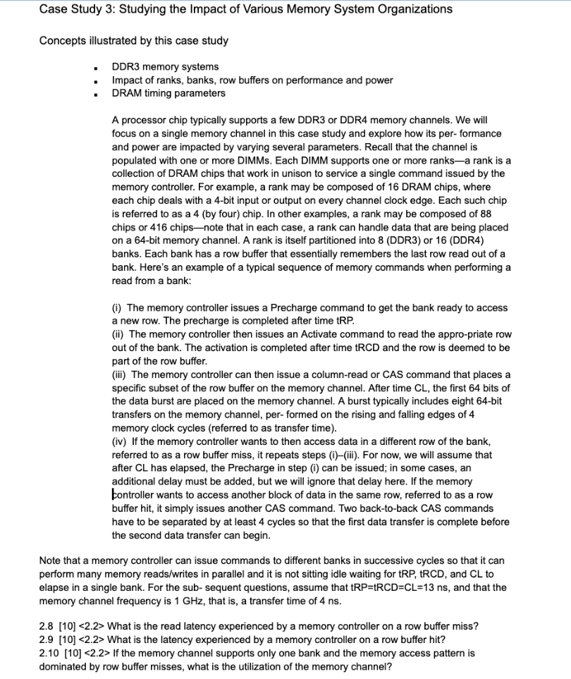
Case Study 3 : Studying the Impact of Various Memory System Organizations Concepts illustrated by this case study DDR 3 memory systems Impact of ranks,
Case Study : Studying the Impact of Various Memory System Organizations
Concepts illustrated by this case study
DDR memory systems
Impact of ranks, banks, row buffers on performance and power
DRAM timing parameters
A processor chip typically supports a few DDR or DDR memory channels. We will
focus on a single memory channel in this case study and explore how its per formance
and power are impacted by varying several parameters. Recall that the channel is
populated with one or more DIMMs. Each DIMM supports one or more ranksa rank is a
collection of DRAM chips that work in unison to service a single command issued by the
memory controller. For example, a rank may be composed of DRAM chips, where
each chip deals with a bit input or output on every channel clock edge. Each such chip
is referred to as a by four chip. In other examples, a rank may be composed of
chips or chipsnote that in each case, a rank can handle data that are being placed
on a bit memory channel. A rank is itself partitioned into DDR or DDR
banks. Each bank has a row buffer that essentially remembers the last row read out of a
bank. Here's an example of a typical sequence of memory commands when performing a
read from a bank:
i The memory controller issues a Precharge command to get the bank ready to access
a new row. The precharge is completed after time tRP
ii The memory controller then issues an Activate command to read the appropriate row
out of the bank. The activation is completed after time TRCD and the row is deemed to be
part of the row buffer.
iii The memory controller can then issue a columnread or CAS command that places a
specific subset of the row buffer on the memory channel. After time CL the first bits of
the data burst are placed on the memory channel. A burst typically includes eight bit
transfers on the memory channel, per formed on the rising and falling edges of
memory clock cycles referred to as transfer time
iv If the memory controller wants to then access data in a different row of the bank,
referred to as a row buffer miss, it repeats steps iiii For now, we will assume that
after CL has elapsed, the Precharge in step i can be issued; in some cases, an
additional delay must be added, but we will ignore that delay here. If the memory
kontroller wants to access another block of data in the same row, referred to as a row
buffer hit, it simply issues another CAS command. Two backtoback CAS commands
have to be separated by at least cycles so that the first data transfer is complete before
the second data transfer can begin.
Note that a memory controller can issue commands to different banks in successive cycles so that it can
perform many memory readswrites in parallel and it is not sitting idle waiting for tRP TRCD and CL to
elapse in a single bank. For the sub sequent questions, assume that and that the
memory channel frequency is that is a transfer time of
What is the read latency experienced by a memory controller on a row buffer miss?
What is the latency experienced by a memory controller on a row buffer hit?
If the memory channel supports only one bank and the memory access pattern is
dominated by row buffer misses, what is the utilization of the memory channel?

Step by Step Solution
There are 3 Steps involved in it
Step: 1

Get Instant Access to Expert-Tailored Solutions
See step-by-step solutions with expert insights and AI powered tools for academic success
Step: 2

Step: 3

Ace Your Homework with AI
Get the answers you need in no time with our AI-driven, step-by-step assistance
Get Started


