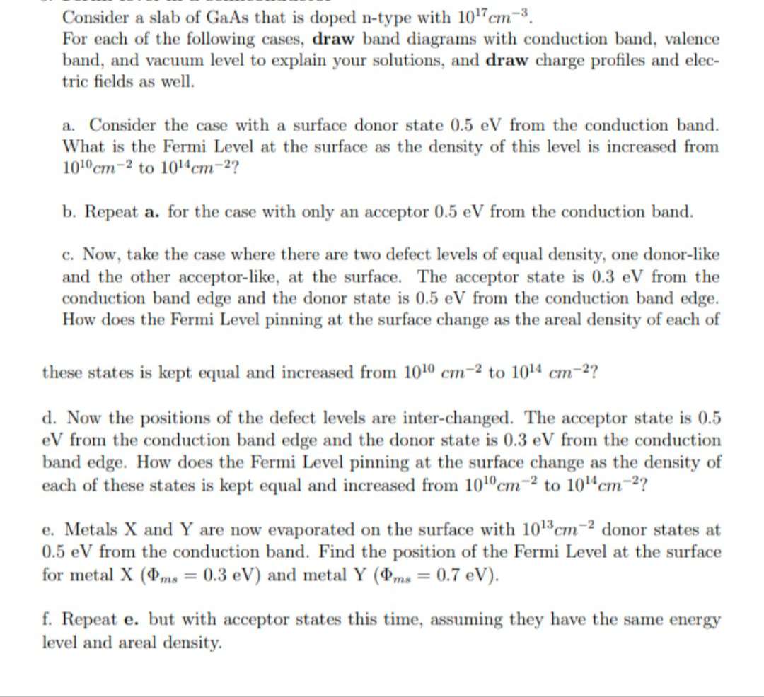
Consider a slab of GaAs that is doped n-type with 10'7cm-3 For each of the following cases, draw band diagrams with conduction band, valence band, and vacuum level to explain your solutions, and draw charge profiles and elec- tric fields as well. a. Consider the case with a surface donor state 0.5 eV from the conduction band. What is the Fermi Level at the surface as the density of this level is increased from 1010cm-2 to 1014cm-2? b. Repeat a. for the case with only an acceptor 0.5 eV from the conduction band. c. Now, take the case where there are two defect levels of equal density, one donor-like and the other acceptor-like, at the surface. The acceptor state is 0.3 eV from the conduction band edge and the donor state is 0.5 eV from the conduction band edge. How does the Fermi Level pinning at the surface change as the areal density of each of these states is kept equal and increased from 1010 cm-2 to 1014 cm-2? d. Now the positions of the defect levels are inter-changed. The acceptor state is 0.5 eV from the conduction band edge and the donor state is 0.3 eV from the conduction band edge. How does the Fermi Level pinning at the surface change as the density of each of these states is kept equal and increased from 100cm-2 to 104cm-2? e. Metals X and Y are now evaporated on the surface with 1013cm-2 donor states at 0.5 eV from the conduction band. Find the position of the Fermi Level at the surface for metal X (m3 = 0.3 eV) and metal Y (oms = 0.7 eV). f. Repeat e. but with acceptor states this time, assuming they have the same energy level and areal density. Consider a slab of GaAs that is doped n-type with 10'7cm-3 For each of the following cases, draw band diagrams with conduction band, valence band, and vacuum level to explain your solutions, and draw charge profiles and elec- tric fields as well. a. Consider the case with a surface donor state 0.5 eV from the conduction band. What is the Fermi Level at the surface as the density of this level is increased from 1010cm-2 to 1014cm-2? b. Repeat a. for the case with only an acceptor 0.5 eV from the conduction band. c. Now, take the case where there are two defect levels of equal density, one donor-like and the other acceptor-like, at the surface. The acceptor state is 0.3 eV from the conduction band edge and the donor state is 0.5 eV from the conduction band edge. How does the Fermi Level pinning at the surface change as the areal density of each of these states is kept equal and increased from 1010 cm-2 to 1014 cm-2? d. Now the positions of the defect levels are inter-changed. The acceptor state is 0.5 eV from the conduction band edge and the donor state is 0.3 eV from the conduction band edge. How does the Fermi Level pinning at the surface change as the density of each of these states is kept equal and increased from 100cm-2 to 104cm-2? e. Metals X and Y are now evaporated on the surface with 1013cm-2 donor states at 0.5 eV from the conduction band. Find the position of the Fermi Level at the surface for metal X (m3 = 0.3 eV) and metal Y (oms = 0.7 eV). f. Repeat e. but with acceptor states this time, assuming they have the same energy level and areal density


