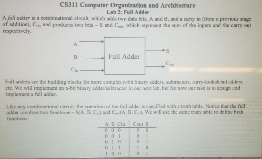
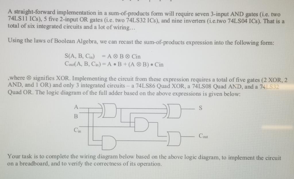
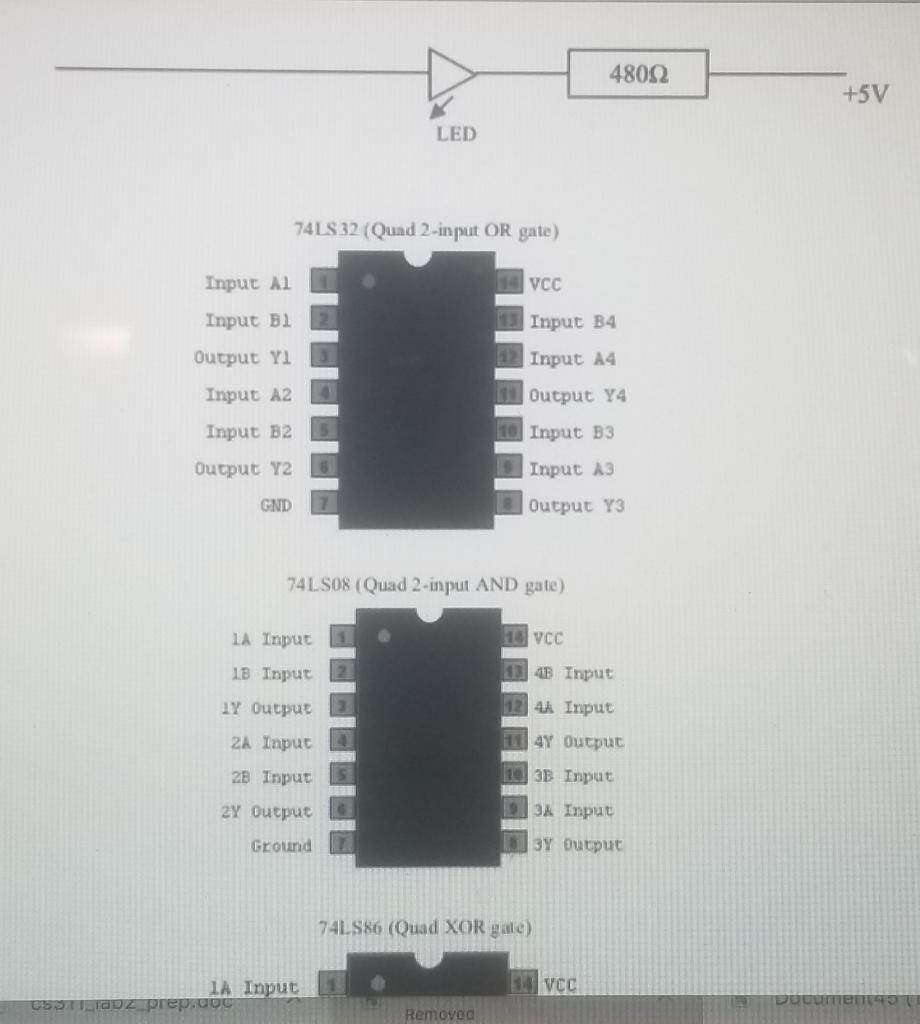
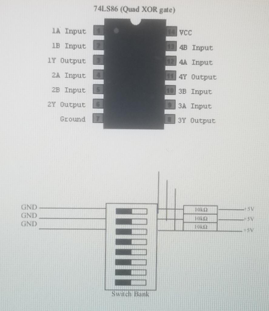
CS311 Computer Organization and Architecture Lab 2: Full Adder A full adder is a combinational circuit, which adds two data bits, A and B, and a carry in (from a previous stage of addition), Cin, and produces two bits - S and Cout, which represent the sum of the inputs and the carry out respectively. A S B Full Adder Cout Cin Full adders are the building blocks for more complex n-bit binary adders, subtractors, carry-lookahead adders, etc. We will implement an n-bit binary adder/subtractor in our next lab, but for now our task is to design and implement a full adder. Like any combinational circuit, the operation of the full adder is specified with a truth table. Notice that the full adder involves two functions - S(A, B, C.) and Cou(A.B.C.). We will use the same truth table to define both functions: A B Cin Couts 0 0 0 0 0 1 0 1 0 0 1 1 1 0 0 0 0 0 1 0 0 1 1 0 1 A straight-forward implementation in a sum-of-products form will require seven 3-input AND gates (i.e. two 74LS11 ICs), 5 five 2-input OR gates (i.e. two 74LS32 ICs), and nine inverters (i.e.two 74LS04 ICs). That is a total of six integrated circuits and a lot of wiring... Using the laws of Boolean Algebra, we can recast the sum-of-products expression into the following form: S(A, B, Cin) = AB Cin Cout(A, B, Cin) = A B +( AB) Cin , where signifies XOR. Implementing the circuit from these expression requires a total of five gates (2 XOR, 2 AND, and 1 OR) and only 3 integrated circuits - a 74LS86 Quad XOR, a 74LS08 Quad AND, and a 74LS32 Quad OR. The logic diagram of the full adder based on the above expressions is given below: s B Cin Coul Your task is to complete the wiring diagram below based on the above logic diagram, to implement the circuit on a breadboard, and to verify the correctness of its operation, 48092 +5V LED 74LS 32 (Quad 2-input OR gate) Input Al vec Input B Input B4 Output y 12 Input A4 Output Y4 Input A2 10 Input B3 Input B2 Output Y2 Input A3 Output Y3 GND ! 74LSOS (Quad 2-input AND gate) 1A Input 1 VCC 1B Input 134B Input 1Y Output 12 4 Input 24 Input 4Y Output 2B Input 3B Input 2Y Output 3x Input 3Y Output Ground 74L 586 (Quad XOR gale) Avec la Input USTADZ prep.co Removed 74LS86 (Quad XOR gate) IA Input VCC 1B Input 4B Input IY Output 12 44 Input 2A Input 13 4Y Output 2B Input 10 3B Input Input 24 Output Ground 3Y Output 10102 SV GND GND CND 5V SV Switch Bank CS311 Computer Organization and Architecture Lab 2: Full Adder A full adder is a combinational circuit, which adds two data bits, A and B, and a carry in (from a previous stage of addition), Cin, and produces two bits - S and Cout, which represent the sum of the inputs and the carry out respectively. A S B Full Adder Cout Cin Full adders are the building blocks for more complex n-bit binary adders, subtractors, carry-lookahead adders, etc. We will implement an n-bit binary adder/subtractor in our next lab, but for now our task is to design and implement a full adder. Like any combinational circuit, the operation of the full adder is specified with a truth table. Notice that the full adder involves two functions - S(A, B, C.) and Cou(A.B.C.). We will use the same truth table to define both functions: A B Cin Couts 0 0 0 0 0 1 0 1 0 0 1 1 1 0 0 0 0 0 1 0 0 1 1 0 1 A straight-forward implementation in a sum-of-products form will require seven 3-input AND gates (i.e. two 74LS11 ICs), 5 five 2-input OR gates (i.e. two 74LS32 ICs), and nine inverters (i.e.two 74LS04 ICs). That is a total of six integrated circuits and a lot of wiring... Using the laws of Boolean Algebra, we can recast the sum-of-products expression into the following form: S(A, B, Cin) = AB Cin Cout(A, B, Cin) = A B +( AB) Cin , where signifies XOR. Implementing the circuit from these expression requires a total of five gates (2 XOR, 2 AND, and 1 OR) and only 3 integrated circuits - a 74LS86 Quad XOR, a 74LS08 Quad AND, and a 74LS32 Quad OR. The logic diagram of the full adder based on the above expressions is given below: s B Cin Coul Your task is to complete the wiring diagram below based on the above logic diagram, to implement the circuit on a breadboard, and to verify the correctness of its operation, 48092 +5V LED 74LS 32 (Quad 2-input OR gate) Input Al vec Input B Input B4 Output y 12 Input A4 Output Y4 Input A2 10 Input B3 Input B2 Output Y2 Input A3 Output Y3 GND ! 74LSOS (Quad 2-input AND gate) 1A Input 1 VCC 1B Input 134B Input 1Y Output 12 4 Input 24 Input 4Y Output 2B Input 3B Input 2Y Output 3x Input 3Y Output Ground 74L 586 (Quad XOR gale) Avec la Input USTADZ prep.co Removed 74LS86 (Quad XOR gate) IA Input VCC 1B Input 4B Input IY Output 12 44 Input 2A Input 13 4Y Output 2B Input 10 3B Input Input 24 Output Ground 3Y Output 10102 SV GND GND CND 5V SV Switch Bank