

Question: Datapath and control unit depicted below used to calculate the Fibonacci series for 4-bits. F(1) = 1, F(2) = 1 and F(N) = F(N-2) +
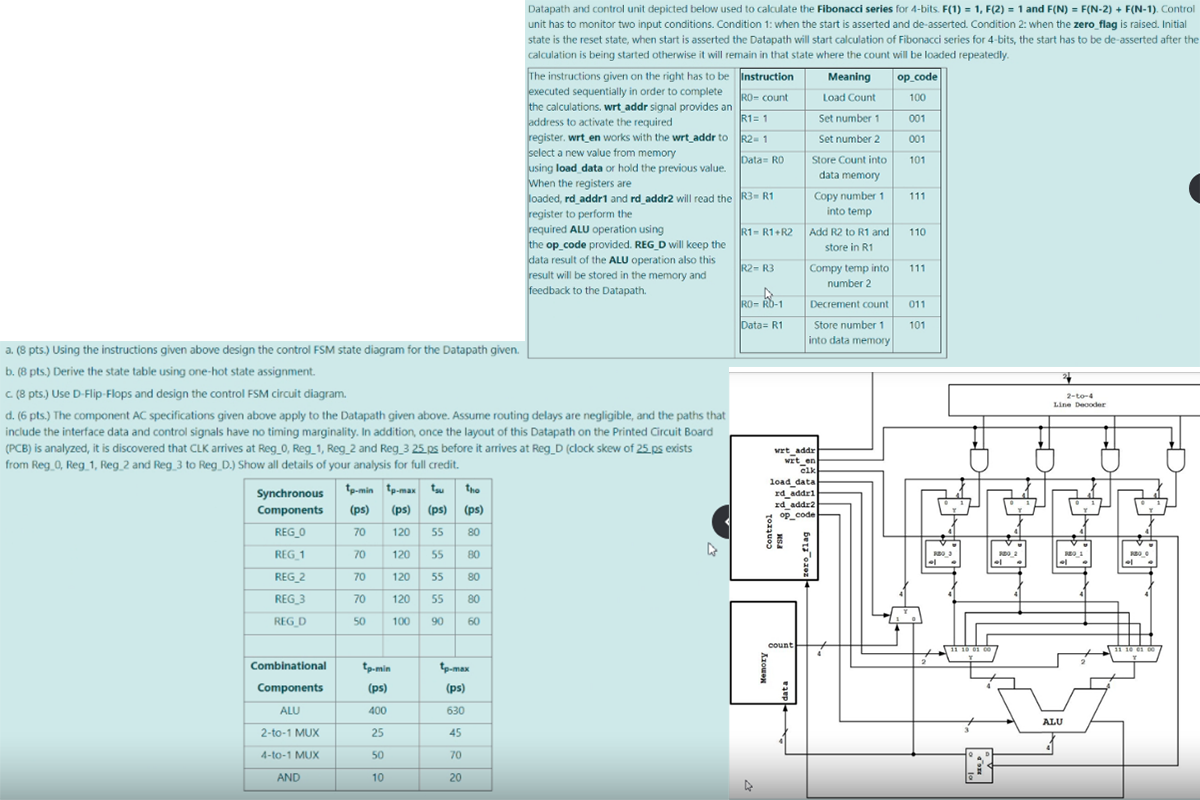
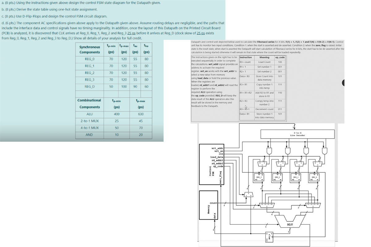
Datapath and control unit depicted below used to calculate the Fibonacci series for 4-bits. F(1) = 1, F(2) = 1 and F(N) = F(N-2) + F(N-1). Control unit has to monitor two input conditions. Condition 1: when the start is asserted and de-asserted. Condition 2: when the zero_flag is raised. Initial state is the reset state, when start is asserted the Datapath will start calculation of Fibonacci series for 4-bits, the start has to be de-asserted after the calculation is being started otherwise it will remain in that state where the count will be loaded repeatedly. The instructions given on the right has to be instruction Meaning op_code executed sequentially in order to complete RO= count Load Count 100 the calculations, wrt addr signal provides an R1 = 1 address to activate the required Set number 1 001 register, wrt_en works with the wrt_addr to R2-1 Set number 2 001 select a new value from memory Data RO Store Count into 101 using load data or hold the previous value. data memory When the registers are Joaded, rd_addr1 and rd addr2 will read the R3-R1 Copy number 1 111 register to perform the into temp required ALU operation using R1 - R1+R2 Add R2 to R1 and 110 the op_code provided. REG D will keep the store in R1 data result of the ALU operation also this R2-R3 Compy temp into 111 result will be stored in the memory and feedback to the Datapath. number 2 2 Decrement count 011 RO-RO-1 Data= R1 101 Store number 1 into data memory 2-to- Line Decoder a. (8 pts. Using the instructions given above design the control FSM state diagram for the Datapath given b. (8 pts) Derive the state table using one-hot state assignment. C (8 pts.) Use D-Flip-Flops and design the control FSM circuit diagram. d. (6 pts.) The component AC specifications given above apply to the Datapath given above. Assume routing delays are negligible, and the paths that include the interface data and control signals have no timing marginality. In addition, once the layout of this Datapath on the Printed Circuit Board (PCB) is analyzed, it is discovered that CLK arrives at Reg_O, Reg_1, Reg_2 and Reg_325.ps before it arrives at Reg_D (clock skew of 25.ps exists from Reg 0, Reg 1, Reg 2 and Reg_3 to Reg D.) Show all details of your analysis for full credit. Synchronous tp-min tp-max tu the Components (ps) (ps) (ps) (ps) REG_0 70 120 55 80 REG 1 70 120 55 80 REG 2 70 120 55 80 wet addr wrt en elk load data rd_addr1 ud addr2 op_code DO 100 a NO 1 MBO be 2011 REG 3 70 120 55 80 REG D 50 100 90 60 count Combinational tp.min (ps) (ps) Components ALU 400 630 ALU 2-to-1 MUX 25 45 4-10-1 MUX 50 70 AND 10 20 a. (8 pts. Using the instructions given above design the control FSM state diagram for the Datapath given. b. (8 pts.) Derive the state table using one hot state assignment. C (8 pts.) Use D Flip-Flops and design the control FSM circuit diagram. - d. (6 pts.) The component AC specifications given above apply to the Datapath given above. Assume routing delays are negligible, and the paths that include the interface data and control signals have no timing marginality. In addition, once the layout of this Datapath on the Printed Circuit Board (PCB) is analyzed, it is discovered that CLK arrives at Reg_0, Reg_1, Reg_2 and Reg_3 25 ps before it arrives at Reg_D (clock skew of 25.ps exists from Reg 0, Reg 1, Reg 2 and Reg_3 to Reg_D.) Show all details of your analysis for full credit. Datapath and control unit depicted below used to calculate the Fibonacci series for 4-bits. F(t) = 1, F(2) = 1 and F(N) = F(N-2) + F(N-1). Control tip-min tp-max to Synchronous the unit has to monitor two input conditions. Condition 1: when the start is asserted and de-asserted Condition 2 when the zero flag is raised. Initial state is the reset state, when start is asserted the Datapath will start calculation of Fibonacci series for 4-bits, the start has to be de-asserted after the Components (ps) (ps) (ps) (ps) Galculation is being started otherwise it will remain in that state where the count will be loaded repeatedly The instructions given on the right has to be instruction 70 REG_0 120 55 Meaning 80 op.code kecuted sequentially in order to complete Roscount Load Count 100 REG 1 70 120 55 80 the calculations. wrt addr signal provides an address to activate the required R1 = 1 Set number 1 001 REG_2 70 120 55 80 register wit en works with the wrt_addr to R2.1 Set number 2 001 select a new value from memory Data RO Store Count into 101 REG 3 70 120 55 80 using load data or hold the previous value. When the registers are data memory REG D 111 50 100 90 loaded, rd addr1 and rd addr2 will read the R3-R1 60 Copy number 1 register to perform the into temp required ALU operation using R1 R1 R2 Add R2 to R1 and 110 the op.code provided. REG D will keep the store in R1 Combinational tp.min to-max data result of the ALU operation also this result will be stored in the memory and 22-R3 Compy temp into 111 number 2 Components feedback to the Datapath (ps) (ps) RO1 Decrement count 011 ALU 400 630 Data R1 Store number 1 101 into data memory 2-to-1 MUX 25 45 4-10-1 MUX 50 70 AND 10 20 1 wrt_adde Et en clk load data Id addr1 rd addr2 op_code count 8 ALU cm Datapath and control unit depicted below used to calculate the Fibonacci series for 4-bits. F(1) = 1, F(2) = 1 and F(N) = F(N-2) + F(N-1). Control unit has to monitor two input conditions. Condition 1: when the start is asserted and de-asserted. Condition 2: when the zero_flag is raised. Initial state is the reset state, when start is asserted the Datapath will start calculation of Fibonacci series for 4-bits, the start has to be de-asserted after the calculation is being started otherwise it will remain in that state where the count will be loaded repeatedly. The instructions given on the right has to be instruction Meaning op_code executed sequentially in order to complete RO= count Load Count 100 the calculations, wrt addr signal provides an R1 = 1 address to activate the required Set number 1 001 register, wrt_en works with the wrt_addr to R2-1 Set number 2 001 select a new value from memory Data RO Store Count into 101 using load data or hold the previous value. data memory When the registers are Joaded, rd_addr1 and rd addr2 will read the R3-R1 Copy number 1 111 register to perform the into temp required ALU operation using R1 - R1+R2 Add R2 to R1 and 110 the op_code provided. REG D will keep the store in R1 data result of the ALU operation also this R2-R3 Compy temp into 111 result will be stored in the memory and feedback to the Datapath. number 2 2 Decrement count 011 RO-RO-1 Data= R1 101 Store number 1 into data memory 2-to- Line Decoder a. (8 pts. Using the instructions given above design the control FSM state diagram for the Datapath given b. (8 pts) Derive the state table using one-hot state assignment. C (8 pts.) Use D-Flip-Flops and design the control FSM circuit diagram. d. (6 pts.) The component AC specifications given above apply to the Datapath given above. Assume routing delays are negligible, and the paths that include the interface data and control signals have no timing marginality. In addition, once the layout of this Datapath on the Printed Circuit Board (PCB) is analyzed, it is discovered that CLK arrives at Reg_O, Reg_1, Reg_2 and Reg_325.ps before it arrives at Reg_D (clock skew of 25.ps exists from Reg 0, Reg 1, Reg 2 and Reg_3 to Reg D.) Show all details of your analysis for full credit. Synchronous tp-min tp-max tu the Components (ps) (ps) (ps) (ps) REG_0 70 120 55 80 REG 1 70 120 55 80 REG 2 70 120 55 80 wet addr wrt en elk load data rd_addr1 ud addr2 op_code DO 100 a NO 1 MBO be 2011 REG 3 70 120 55 80 REG D 50 100 90 60 count Combinational tp.min (ps) (ps) Components ALU 400 630 ALU 2-to-1 MUX 25 45 4-10-1 MUX 50 70 AND 10 20 a. (8 pts. Using the instructions given above design the control FSM state diagram for the Datapath given. b. (8 pts.) Derive the state table using one hot state assignment. C (8 pts.) Use D Flip-Flops and design the control FSM circuit diagram. - d. (6 pts.) The component AC specifications given above apply to the Datapath given above. Assume routing delays are negligible, and the paths that include the interface data and control signals have no timing marginality. In addition, once the layout of this Datapath on the Printed Circuit Board (PCB) is analyzed, it is discovered that CLK arrives at Reg_0, Reg_1, Reg_2 and Reg_3 25 ps before it arrives at Reg_D (clock skew of 25.ps exists from Reg 0, Reg 1, Reg 2 and Reg_3 to Reg_D.) Show all details of your analysis for full credit. Datapath and control unit depicted below used to calculate the Fibonacci series for 4-bits. F(t) = 1, F(2) = 1 and F(N) = F(N-2) + F(N-1). Control tip-min tp-max to Synchronous the unit has to monitor two input conditions. Condition 1: when the start is asserted and de-asserted Condition 2 when the zero flag is raised. Initial state is the reset state, when start is asserted the Datapath will start calculation of Fibonacci series for 4-bits, the start has to be de-asserted after the Components (ps) (ps) (ps) (ps) Galculation is being started otherwise it will remain in that state where the count will be loaded repeatedly The instructions given on the right has to be instruction 70 REG_0 120 55 Meaning 80 op.code kecuted sequentially in order to complete Roscount Load Count 100 REG 1 70 120 55 80 the calculations. wrt addr signal provides an address to activate the required R1 = 1 Set number 1 001 REG_2 70 120 55 80 register wit en works with the wrt_addr to R2.1 Set number 2 001 select a new value from memory Data RO Store Count into 101 REG 3 70 120 55 80 using load data or hold the previous value. When the registers are data memory REG D 111 50 100 90 loaded, rd addr1 and rd addr2 will read the R3-R1 60 Copy number 1 register to perform the into temp required ALU operation using R1 R1 R2 Add R2 to R1 and 110 the op.code provided. REG D will keep the store in R1 Combinational tp.min to-max data result of the ALU operation also this result will be stored in the memory and 22-R3 Compy temp into 111 number 2 Components feedback to the Datapath (ps) (ps) RO1 Decrement count 011 ALU 400 630 Data R1 Store number 1 101 into data memory 2-to-1 MUX 25 45 4-10-1 MUX 50 70 AND 10 20 1 wrt_adde Et en clk load data Id addr1 rd addr2 op_code count 8 ALU cm
Step by Step Solution
There are 3 Steps involved in it

Get step-by-step solutions from verified subject matter experts