

Question
DATAPATH MODULE - TESTBENCH & FUNCTIONAL VERIFICATION The following are the main task of datapath unit that has to be behaviourally model by verilog code
DATAPATH MODULE - TESTBENCH & FUNCTIONAL VERIFICATION
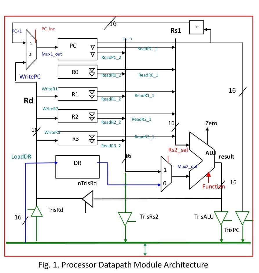
The following are the main task of datapath unit that has to be behaviourally model by verilog code to suit the definition of design processor as can be view in figure 1: 1. To model the read operation for both Rs1 (source1 register) and Rs2 (source2 register) from any one of 5 available register (R0, R1, R2, R3, PC). 2. To model the write operation for Rd (destination register) from any one of 4 available register (R1, R2, R3, PC). 3. To model the tri-state buffer (TrisALU, TrisPC, TrisRs2, TrisRd) for system bus.
Experiment #1 Datapath Module 1. Create datapath.v in a text editor using the following Verilog Code and add into Project.
THE CODE `include "opcodes.v" `timescale 100ps / 10ps module datapath( Sysbus, Zero, Function, TrisALU, TrisPC, TrisRs2, TrisRd, nTrisRd, Clock, nReset, ReadPC_1, ReadPC_2, ReadR0_1, ReadR0_2, ReadR1_1, PC_inc, ReadR1_2, ReadR2_1, ReadR2_2, ReadR3_1, ReadR3_2, PC_inc, WriteR1, WriteR2, WriteR3, Rs2_sel, LoadDR, LoadPC); inout [15:0] Sysbus; output Zero; input [2:0] Function; input TrisALU, TrisPC, TrisRs2, TrisRd, nTrisRd, Rs2_sel, ReadPC_1, ReadPC_2, ReadR0_1, ReadR0_2, ReadR1_1, ReadR1_2, ReadR2_1, ReadR2_2, ReadR3_1, ReadR3_2, PC_inc, WriteR1, WriteR2, WriteR3, LoadDR, LoadPC; input Clock, nReset; reg [15:0] PC, R1, R2, R3, R0, DR; wire Zero; wire [15:0] Rd, Rs1, Rs2, result; wire [15:0] Mux2_out, Mux1_out; assign Rs1 = ( ReadPC_1) ? PC : 16'bz; assign Rs1 = ( ReadR0_1) ? R0 : 16'bz; assign Rs1 = ( ReadR1_1) ? R1 : 16'bz; assign Rs1 = ( ReadR2_1) ? R2 : 16'bz; assign Rs1 = ( ReadR3_1) ? R3 : 16'bz; assign Rs2 = ( ReadPC_2) ? PC : 16'bz; assign Rs2 = ( ReadR0_2) ? R0 : 16'bz; assign Rs2 = ( ReadR1_2) ? R1 : 16'bz; assign Rs2 = ( ReadR2_2) ? R2 : 16'bz; assign Rs2 = ( ReadR3_2) ? R3 : 16'bz; alu ALU ( alu_Zero, result, Rs1, Mux2_out, Function); always @(posedge Clock) begin if (LoadPC) PC = Mux1_out; if (WriteR1) R1 = Rd; if (WriteR2) R2 = Rd; if (WriteR3) R3 = Rd; if (LoadDR) DR = Sysbus; end assign Mux2_out = ( Rs2_sel ) ? Rs2 : DR; assign Zero = (result == 0); assign Mux1_out = ( PC_inc ) ? PC + 1 : Rd; assign Rd = (TrisRd ) ? Sysbus : 16'bz; assign Rd = (nTrisRd) ? result : 16'bz; assign Sysbus = ( TrisALU ) ? result : 16'bz; assign Sysbus = ( TrisPC ) ? PC : 16'bz; assign Sysbus = ( TrisRs2) ? Rs2 : 16'bz; always @(nReset) if (!nReset) begin assign PC = 0; assign R1 = 0; assign R2 = 0; assign R3 = 0; assign DR = 0; assign R0 = 0; end else begin deassign PC; deassign R1; deassign R2; deassign R3; deassign DR; end endmodule
2. Save the Verilog Code. 3. Right click on the Project Window and select Add to Project to Existing File 4. Browse your File and Select Copy to Project Directory at the bottom then click OK. 5. Select the file and compile it. Experiment #2 Test bench and analysis of Datapath Module 1. Create a test bench to verify the functionality of datapath module and save it as datapath_tst.v. 2. Select all the files and compile it. 3. Select the test bench and simulate it. 4. Add Waveform to the window and then verify the design. Save the waveform in Drawing Tools Software. Include all results in your report. 5. From the waveform obtained, analyze the functionality of control unit based on the Computer Architecture Theory. 6. Describe and discuss any problems encountered of the design.
Step by Step Solution
There are 3 Steps involved in it
Step: 1

Get Instant Access to Expert-Tailored Solutions
See step-by-step solutions with expert insights and AI powered tools for academic success
Step: 2

Step: 3
Ace Your Homework with AI
Get the answers you need in no time with our AI-driven, step-by-step assistance
Get Started
Databases In Networked Information Systems Second International Workshop Dnis 2002 Aizu Japan December 18 2002 Proceeding Lncs 2544
Authors: Subash Bhalla
1st Edition
3540002642, 978-3540002642