 ddidn't do this lab correctly but we don't get a solution so I don't know what the circuit looks like correctly.
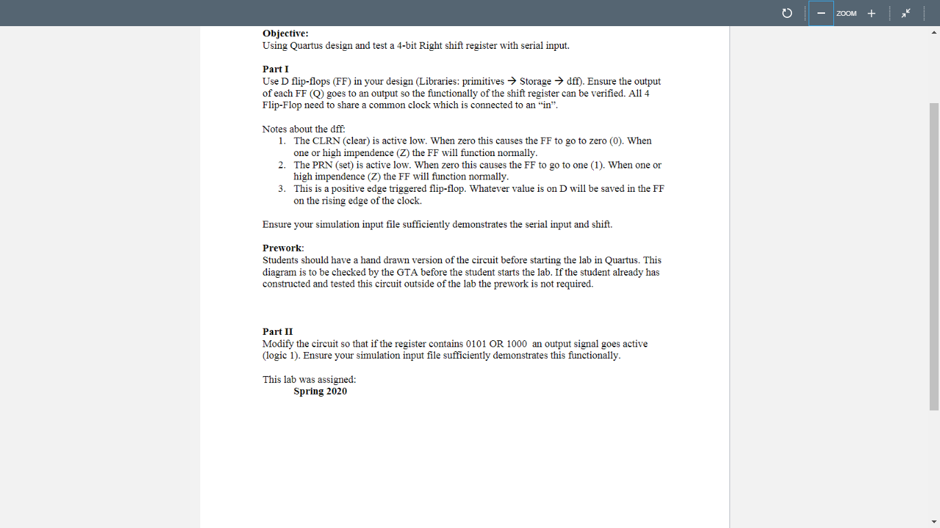
ZOOM + 1 Objective: Using Quartus design and test a 4-bit Right shift register with serial input. Part I Use D flip-flops (FF) in your design (Libraries: primitives Storage dff). Ensure the output of each FF (O goes to an output so the functionally of the shift register can be verified. All 4 Flip-Flop need to share a common clock which is connected to an "in". Notes about the dff: 1. The CLRN (Clear) is active low. When zero this causes the FF to go to zero (O). When one or high impendence (Z) the FF will function normally. 2. The PRN (set) is active low. When zero this causes the FF to go to one (1). When one or high impendence (Z) the FF will function normally. 3. This is a positive edge triggered flip-flop. Whatever value is on D will be saved in the FF on the rising edge of the clock. Ensure your simulation input file sufficiently demonstrates the serial input and shift. Prework: Students should have a hand drawn version of the circuit before starting the lab in Quartus. This diagram is to be checked by the GTA before the student starts the lab. If the student already has constructed and tested this circuit outside of the lab the prework is not required. Part II Modify the circuit so that if the register contains 0101 OR 1000 an output signal goes active (logic 1). Ensure your simulation input file sufficiently demonstrates this functionally. This lab was assigned: Spring 2020 ZOOM + 1 Objective: Using Quartus design and test a 4-bit Right shift register with serial input. Part I Use D flip-flops (FF) in your design (Libraries: primitives Storage dff). Ensure the output of each FF (O goes to an output so the functionally of the shift register can be verified. All 4 Flip-Flop need to share a common clock which is connected to an "in". Notes about the dff: 1. The CLRN (Clear) is active low. When zero this causes the FF to go to zero (O). When one or high impendence (Z) the FF will function normally. 2. The PRN (set) is active low. When zero this causes the FF to go to one (1). When one or high impendence (Z) the FF will function normally. 3. This is a positive edge triggered flip-flop. Whatever value is on D will be saved in the FF on the rising edge of the clock. Ensure your simulation input file sufficiently demonstrates the serial input and shift. Prework: Students should have a hand drawn version of the circuit before starting the lab in Quartus. This diagram is to be checked by the GTA before the student starts the lab. If the student already has constructed and tested this circuit outside of the lab the prework is not required. Part II Modify the circuit so that if the register contains 0101 OR 1000 an output signal goes active (logic 1). Ensure your simulation input file sufficiently demonstrates this functionally. This lab was assigned: Spring 2020
 ddidn't do this lab correctly but we don't get a solution so I don't know what the circuit looks like correctly.


