Question
Description : - Simulate the example shown above in Proteus and visualize the results. Describe the limitations of LM35 in Proteus for visualisation of the
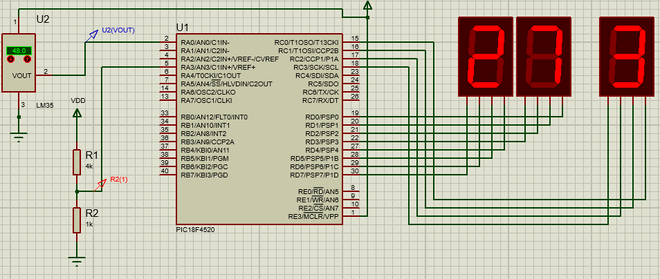
Description : - Simulate the example shown above in Proteus and visualize the results. Describe the limitations of LM35 in Proteus for visualisation of the result. - Increase the resolution of your system by using an external reference voltage of 1v for ADC. This can be done by connecting the output voltage of a voltage divider circuit as shown below. (you need to use ADC_VREFPLUS_EXT for open ADC parameter.)
- Calculate the new resolution. - Change the code to calculate the temperature based on new resolution. - Observe and describe the changes compared to the low resolution circuit and also the limitations in simulation environment. - Include snapshots of your simulation in your report.
At the bottom, here's an example of a circuit and its working code on Proteus. We have to convert that circuit into 2nd circuit and we have to make the right adjustments for the code. So, what is the right code for the 2nd circuit ? And please describe the changes compared to the low resolution circuit and also the limitations in simulation environment.
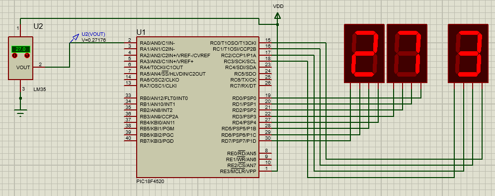
Example: Connect an analogue temperature sensor (LM35) to PIC and convert the analogue voltage from sensor into a digital value. Knowing every 1 C makes 10 mv change in the sensor output voltage, show two digits of temperature on two 7 segments connected to PORTD and show one digit after decimal point on a third 7segment attached in port C. (use Vref ++=5v and Vref --=0v , right justification and AN0 for the ADC converter

- 1st circuit -
Its working code :
/* ADC Interfacing example for 10-bit ADC*/ /* The following example shows the procedure of setting up and using the PIC ADC */ /* PIC ADC Ch 0 is used as the Analogue i/p. */
#pragma config OSC = HS /* set osc mode to HS */ #pragma config WDT = OFF /* set watchdog timer off */ #pragma config LVP = OFF /* Low Voltage Programming Off */ #pragma config DEBUG = OFF /* Compile without extra Debug compile Code */
#include
char dig1, dig2,dig3,rem; float result; unsigned int intextract;
void main (void) { LATD=0 ;
TRISA = 0xFF; /* Configure Port A as I/Ps for ADC */ TRISD = 0X00; /* Configure Port D as all O/P */ TRISC = 0X00; /* Configure the ADC */ /* The following configure the ADC module operational mode */ /* OpenADC configures the operation of the ADC with a number of arguments */ /* ADC_FOSC selects the ADC clock source and has a number of set values */ /* ADC_RIGHT_JUST select ADC result justification */ /* ADC_0_TAD sets the A/D acquisition time select */ /* ADC_CH0 select Channel 0 */ /* ADC_INT_OFF Interrupts are disabled */ /* ADC_VREFPLUS_VDD set ADC + reference voltage configuration to VDD */ /* ADC_VREFMINUS_VSS set ADC - reference voltage configuration to VSS */ /* 0b1011 are the A/D control Register 1 config bits setting the reference and function of port bits */ while (1) { OpenADC(ADC_FOSC_32 & ADC_RIGHT_JUST & ADC_20_TAD,ADC_CH0 & ADC_INT_OFF & ADC_VREFPLUS_VDD & ADC_VREFMINUS_VSS, 0b1011); ConvertADC( ); /* start A/D conversion */ while(BusyADC( )); /* wait for completion */ result = ReadADC(); // Read ADC works only for RIGHT
CloseADC( );
/* For LM35 sensor, every 0.01V change is equivalent to 1 Celsius degree change. So if 5V is equivalent to 1023 ADC output, then 0.01V change (i.e. 1 degree change) is equivalent to 2.046 ADC output change. Therefore if ADC output is divided by 2.046, we will obtain the degree. */ result = result / 2.046; result=result*10; // to extract one digit after decimal point, the tempreature is multiplied by 10 first. E.G. TEMP=23.51, multiplication by 10 makes it 235.1 intextract=result; // conversion from float type into int type dig1= intextract / 100; // e.g. 235/100=2 rem = intextract % 100;// e.g. 235%100=35 dig2=rem /10;//e.g. 35/10=3 dig3=rem % 10;// e.g. 35%10=5
LATD = (dig1

- 2nd circuit -
VDD 4 1 U2 U2(VOUT) V V=0.27176 27.0 2 VOUT U1 2 15 RAD/AID/C1I- RCO/T10SO/T13CKI 3 RA1/AN1/C2IN- RC1/T10SI/CCP2B 16 4 17 RAZIAN2/C2IN+/VREF-ICVREF 5 RC2/CCP1/P1A 18 6 RA3/AN3/C1IN+/VREF+ RC3/SCKISCL RA4/TOCKI/C1OUT 7 RC4/SDISDA 23 RA5/AN4/SS/HLVDIN/C2OUT 24 14 RC5/SDC 25 RAB/OSC2/CLKO RCB/TX/CK 13 28 RA7/OSC1/CLKI RC7/RX/DT 33 19 RBO/AN12/FLTO/INTO RDO/PSPO 34 20 RB1/AN10/INT1 RD1/PSP1 35 21 RB2/ANS/INT2 RD2/PSP2 38 RB3/AN/CCP2A RD3/PSP3 22 37 27 RB4/KBIO/AN 11 38 RD4/PSP4 RB5/KBI1/PGM 28 RD5/PSP5/P1B 30 RB6/KB12/PGC RD6/PSP/P1C 29 40 RB7KB13/PGD 30 RD7/PSP7/P1D 3 LM35 REO/RD/AN5 RE1/WRIANG RE2/CSIAN RE3/MCLR/VPP 8 9 10 1 PIC18F4520 1 U2 U2(VOUT) U1 48.0 2 3 4 5 6 7 14 13 15 16 17 18 23 24 25 28 RAOIANO/C1IN- RCO/T1OSO/T13CKI RA1/AN1/C2IN- RC1/T10SI/CCP2B RAZIAN2/C2IN+AVREF-ICVREF RC2/CCP1/P1A RA3/AN3/C1IN+/VREF+ RC3/SCKISCL RA4/TOCKI/C1OUT RC4/SD/SDA RA5/AN4/SS/HLVDIN/C2OUT RC5/SDO RAB/OSC2/CLKO RCB/TX/CK RA7/OSC1/CLKI RC7/RXIDT 2 VOUT VDD 3 LM35 4 33 34 35 38 37 38 39 40 RBOVAN12/FLTO/INTO RB1/AN10/INT1 RB2/ANS/INT2 RB3/AN9/CCP2A RB4/KBIO/AN11 RB5/KBI 1/PGM RBO/KBI2/PGC RE7EE13/PGD RDO/PSPO RD1/PSP1 RD2/PSP2 RD3/PSP3 RD4/PSP4 RD5/PSP5/P1B RDB/PSPB/P1C RD7/PSP7/P1D 19 20 21 22 27 28 29 30 R1 4k R2(0) REO/RDIANS RE 1/WR/ANG RE2/CS/AN7 RE3/MCLR/VPP 8 9 10 1 R2 1k PIC18F4520
Step by Step Solution
There are 3 Steps involved in it
Step: 1

Get Instant Access to Expert-Tailored Solutions
See step-by-step solutions with expert insights and AI powered tools for academic success
Step: 2

Step: 3

Ace Your Homework with AI
Get the answers you need in no time with our AI-driven, step-by-step assistance
Get Started


