

Question: Description The purpose of the data unit is to read the words stored in the memory RAM and extract status signals such as the opcode,
Description
The purpose of the data unit is to read the words stored in the memory RAM and extract status signals such as the opcode, address, and flags listed below and send them to the control unit. In addition, it also executes the control signals received from the control unit such as register load, memory readwrite and arithmetic, logic, and shift unit ALU operations. The Data Unit will send to the Control unit the status signals which include the machine instructions bits which have the opcode indirect bit, address bits, and the status flags Z I, N S K M ROM can be used to control memory. The Control Unit will receive the status signals and will produce the sequences of the control signals the control unit will decode the microinstructions into microoperations and will send it to the Data Unit.
The Data Unit works as a medium between the IO interface and the Control Unit; The IO is only connected to the Data Unit. The Control Unit does not have direct access to the IO interface, it gets the IO information from the Data Unit. The Control Unit will produce all the desired control signals which correspond to different microoperations that need to be executed using the status signals address bits, opcode, flags which are provided via the connection between the Control Unit and Data Unit.
Central Processing Unit As shown in the figure, the CPU consists of a control unit and a data unit.
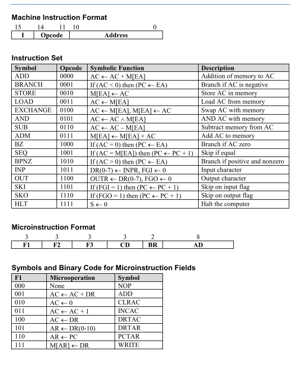
The control unit produces sequences of control signals that correspond to the different microoperations that need to execute, such as register load, register increment, register clear, memory read, memory write, ALU operation selection, etc. These control signals are generated by using the status signals provided by the data unit. The status signals include the machine instruction bits composed of the opcode, indirect bit, and the address bits and status flag bits, such as Z I, N S FGI and FGO.
The control unit includes: Control memory: x Control address register CAR: bits. Subroutine register SBR: bits. Counter to build the timing circuit. Decoders to decode microinstruction control word into microoperations. Logic circuit to generate the control signals.While the data unit includes:
Registers: Address register AR: bits. Program counter PC: bits. Data register DR: bits. Accumulator AC: bits. Input register INPR: bits. Its input is connected to the IO interface module that is connected to the input device, and its output is connected to DR
Output register OUTR: bits. DR and its output is connected to the IO interface module that is connected to the output device.
Flags all are bit in size: Zero flag Z: Z if AC ; Z otherwise. Negative flag N: N if AC; N otherwise. Indirect flag I: I if DR; I otherwise. Input flag FGI: FGI if INPR is empty and ready to receive data from an input device. Output flag FGO: FGO if OUTR is empty and ready to receive data from DR to be sent to an output device.
StartStop flag S: if S stop execution of programs; otherwise allow execution. S is initialized to
Arithmetic, logic, and shift unit: it is responsible for performing arithmetic, logic, and shift operations.
IO Interface Module and InputOutput devices: The IO interface module can be implemented using a buffer of size x This means that it has registers each with bits. The IO interface module can control the inputoutput data transfer operations by the shown control signals, such as input ready, output ready, insert, and delete.
The CPU is connected to the input and output devices via the IO interface modules. The figure shows the data lines and control lines used in the connection.
Instruction Set and Detailed Architecture:
The Appendix includes the details of the instruction set and the architecture that needs to be designed and simulated. You can see that the instruction set is different from that presented in the textbook. Moreover, the computer hardware configuration is slightly different from Chapter as it has more registers such as INPR and OUTR and more flags such as S N FGI, FGO, etc.
Computer Hardware Configuration
Step by Step Solution
There are 3 Steps involved in it
1 Expert Approved Answer
Step: 1 Unlock

Question Has Been Solved by an Expert!
Get step-by-step solutions from verified subject matter experts
Step: 2 Unlock
Step: 3 Unlock