

Question: [3+4 Points]. A CPU (Big Endian named as UC-CS-SS2011) with a single 8-bit-wide bus, 8 bit registers (Program Counter PC, Address Register AR, Data Register
[3+4 Points]. A CPU (Big Endian named as UC-CS-SS2011) with a single 8-bit-wide bus, 8 bit registers (Program Counter PC, Address Register AR, Data Register DR, Accumulator AC, Instruction Register IR) and the 256 X 8 bit RAM memory (Byte addressable) is controlled by 14 control signals (see figure 1 below).
Most of the registers have Load (L) and Enable (E) signals. An active L signal to a register causes the contents of the bus to be clocked into register on the next rising pulse from the system clock, and E does vice versa (Registers, RAM and ALU are clocked). ALU is capable of (i) adding 8-bit numbers contained in two registers AC and DR, (ii) incrementing (AC), and (iii) complementing (AC). In all cases (i)-(iii) the result is saved to AC implicitly. The operations performed by the ALU are selected by the Add (A), Increment (I) and Complement (C) control signals. The accumulator also contains a single flip-flop P that is set whenever its contents are positive (i.e., whenever the leading bit is zero). IP signal on PC increments it by 1.
![[3+4 Points]. A CPU (Big Endian named as UC-CS-SS2011) with a single](https://dsd5zvtm8ll6.cloudfront.net/si.experts.images/questions/2024/09/66f304f7a9b9b_55166f304f73868e.jpg)
The RAM is accessed by first placing the 8-bit address in the Address Register (AR). Then an active Read (R) control signal to the RAM will cause the selected Byte from the RAM to appear on the bus. An active Write (W) signal, on the other hand, will cause the Byte on the bus to be stored in the RAM at the address specified by the AR.
The instructions in this computer are variable length (1 Byte [8-bit OPCODE only] and 2 Byte[8-bit OPCODE and 8-bit ADDRESS]). Opcode specifies the action to be taken for Zero or One address instructions, and the other Byte, when present (for 1 address instructions) indicates the memory address. The list of instructions and their opcodes is given in the figure 2 below.
Control Signal Order (14-bits) in Microcode= LP, EP, IP, LA, R, W, LD, ED, A, I, C, LAC, EAC, LI
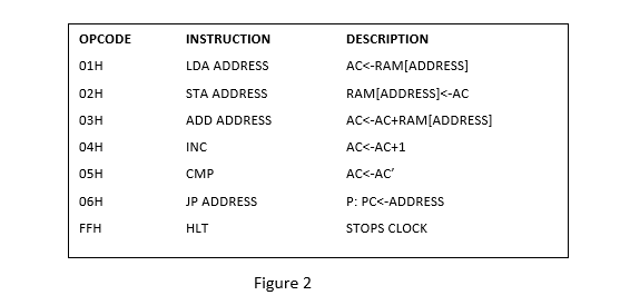
- Write micro-steps for all six instructions given in its Instruction Set.
OR
- Write Boolean Expressions for LA, LD and LAC for hardwired control.
- The micro-programmed Control Unit has the following Microinstruction fields [14 Control Signals, CD (1 bit), MAP or IR (1 bit), HLT (1 bit), Control ROM Jump Address CRJA within the Microcode (5 bits)]. Develop microcode (in Hexadecimal) for Fetch, LDA ADDRESS, STA ADDRESS and JP ADDRESS.
LP EP IP PC (8 bits) B LA - AR (8 bits) U S ADDRESS DATA R RAM=256B 00 W LD B DR (8 bits) ED 1 T LAC EAC S AC (8 bits) W ALU IR (8 bits) D T P LIR H CLK CONTROL UNIT HLT 14 CONTROL SIGNALS Figure 1 OPCODE DESCRIPTION 01H INSTRUCTION LDA ADDRESS STA ADDRESS ADD ADDRESS 02H 03H 04H AC
Step by Step Solution
There are 3 Steps involved in it

Get step-by-step solutions from verified subject matter experts