

Question: Design a combinational circuit that takes 4 bits (X3 X2 X1 X0 ) as inputs, the output will be the result of multiplying the input
Design a combinational circuit that takes 4 bits (X3 X2 X1 X0 ) as inputs, the output will be the result of multiplying the input X by 2. Implement the design using Verilog and verify using waveform. The operation * is not accepted in the solution.
Help please solve operation2 asap
I need the truth table SOP for each output
Kmaps and min SOP for each output
Verilog code
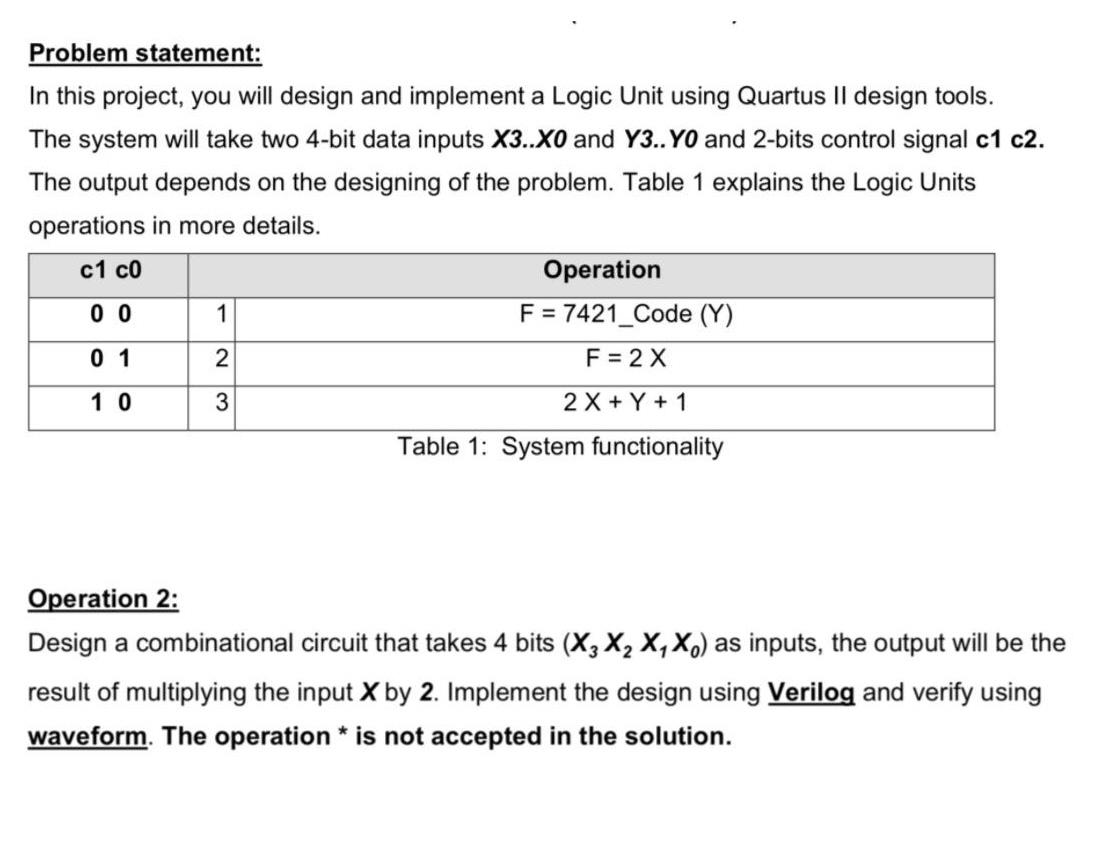
Problem statement: In this project, you will design and implement a Logic Unit using Quartus II design tools. The system will take two 4-bit data inputs X3..XO and Y3.. YO and 2-bits control signal c1 c2. The output depends on the designing of the problem. Table 1 explains the Logic Units operations in more details. c1 co Operation 00 1 F = 7421_Code (Y) 0 1 F = 2 X 10 2 X + Y + 1 Table 1: System functionality 2 3 Operation 2: Design a combinational circuit that takes 4 bits (X, X, X, X) as inputs, the output will be the result of multiplying the input X by 2. Implement the design using Verilog and verify using waveform. The operation * is not accepted in the solution
Step by Step Solution
There are 3 Steps involved in it

Get step-by-step solutions from verified subject matter experts