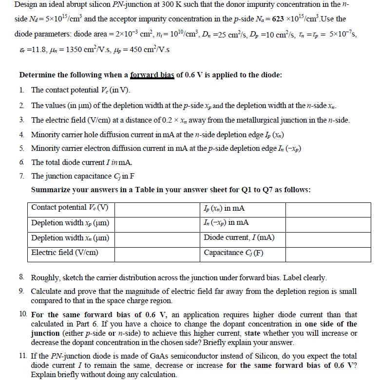
Design an ideal abrupt silicon PN-junction at 300 K such that the donor impurity concentration in the n- side Na=5*10/cm' and the acceptor impurity concentration in the p-side Na=623 x10-5/cm.Use the diode parameters: diode area = 2x10⁻³ cm, n;= 100/cm?, Du =25 cm/s, Dr =10 cmls, In = tp = 5*10-7s, &=11.8, kn = 1350 cm?/V.s, llp = 450 cm?/V.s Determine the following when a forward bias of 0.6 V is applied to the diode: 1. The contact potential V. (in V). 2. The values (in um) of the depletion width at the p-side Xp and the depletion width at the n-side Xn- 3. The electric field (V/cm) at a distance of 0.2 x Xy away from the metallurgical junction in the n-side. 4. Minority carrier hole diffusion current in mA at the n-side depletion edge 1, (Xn) 5. Minority carrier electron diffusion current in mA at the p-side depletion edge In (-Xp) 6. The total diode current I inmA. 7. The junction capacitance C; in F Summarize your answers in a Table in your answer sheet for Q1 to Q7 as follows: Contact potential V. (V) 1. (Xn) in ma Depletion width Xp (um) In (-Xp) in ma Depletion width xn (um) Diode current, I (mA) Electric field (V/cm) Capacitance C(F) & Roughly, sketch the carrier distribution across the junction under forward bias. Label clearly. 9. Calculate and prove that the magnitude of electric field far away from the depletion region is small compared to that in the space charge region. 10. For the same forward bias of 0.6 V, an application requires higher diode current than that calculated in Part 6. If you have a choice to change the dopant concentration in one side of the junction (either p-side or n-side) to achieve this higher current state whether you will increase or decrease the dopant concentration in the chosen side? Briefly explain your answer. 11. If the PN-junction diode is made of GaAs semiconductor instead of Silicon, do you expect the total diode current I to remain the same, decrease or increase for the same forward bias of 0.6 V? Explain briefly without doing any calculation. Design an ideal abrupt silicon PN-junction at 300 K such that the donor impurity concentration in the n- side Na=5*10/cm' and the acceptor impurity concentration in the p-side Na=623 x10-5/cm.Use the diode parameters: diode area = 2x10⁻³ cm, n;= 100/cm?, Du =25 cm/s, Dr =10 cmls, In = tp = 5*10-7s, &=11.8, kn = 1350 cm?/V.s, llp = 450 cm?/V.s Determine the following when a forward bias of 0.6 V is applied to the diode: 1. The contact potential V. (in V). 2. The values (in um) of the depletion width at the p-side Xp and the depletion width at the n-side Xn- 3. The electric field (V/cm) at a distance of 0.2 x Xy away from the metallurgical junction in the n-side. 4. Minority carrier hole diffusion current in mA at the n-side depletion edge 1, (Xn) 5. Minority carrier electron diffusion current in mA at the p-side depletion edge In (-Xp) 6. The total diode current I inmA. 7. The junction capacitance C; in F Summarize your answers in a Table in your answer sheet for Q1 to Q7 as follows: Contact potential V. (V) 1. (Xn) in ma Depletion width Xp (um) In (-Xp) in ma Depletion width xn (um) Diode current, I (mA) Electric field (V/cm) Capacitance C(F) & Roughly, sketch the carrier distribution across the junction under forward bias. Label clearly. 9. Calculate and prove that the magnitude of electric field far away from the depletion region is small compared to that in the space charge region. 10. For the same forward bias of 0.6 V, an application requires higher diode current than that calculated in Part 6. If you have a choice to change the dopant concentration in one side of the junction (either p-side or n-side) to achieve this higher current state whether you will increase or decrease the dopant concentration in the chosen side? Briefly explain your answer. 11. If the PN-junction diode is made of GaAs semiconductor instead of Silicon, do you expect the total diode current I to remain the same, decrease or increase for the same forward bias of 0.6 V? Explain briefly without doing any calculation


