Answered step by step
Verified Expert Solution
Link Copied!

Question

1 Approved Answer

Design diffusion processes to cr eate a pnp bipolar transistor shown in Fig. 3(a): Assume that you start with a p-doped Si wafer with a

Design diffusion processes to cr eate a pnp bipolar transistor shown in Fig. 3(a): Assume that you start with a p-doped Si wafer with a background Aluminum (Al - p-type) dopant concentration of Csub = 5 1016 cm-3 . You try to cre ate a pnp structure by first doping with Arsenic (As - n-type) and then Boron (B - p-type). In the first process, the surface concentration of As is held constant at a value of Cs1= 5 1019 cm-3 . In the second process, the surface concentration of B is held constant at a value of Cs2 = 3 1020 cm-3 . The final pnp junction has both p+ and n+ regions with thicknesses of 1 ?m each, as shown in Fig. 2(a). a) Calculate and draw the final dopant concentration profiles of Al, As, and B as a function of depth (x) to the surface. Labels dopant types, surface concentrations, junction thicknesses, and Csub in your figure. Draw three curves with clear labeling in the figure. Note: for simplicity, at the pn junction interface, we can ignore the third doping concentration, which is more than one order of magnitude lower. (20 points) b) Based on the results in a), calculate and draw the net dopant concentration as a function of depth x, with clear labeling of net dopant types in each region, surface concentrations, junction thicknesses, and Csub in your figure. (10 points)
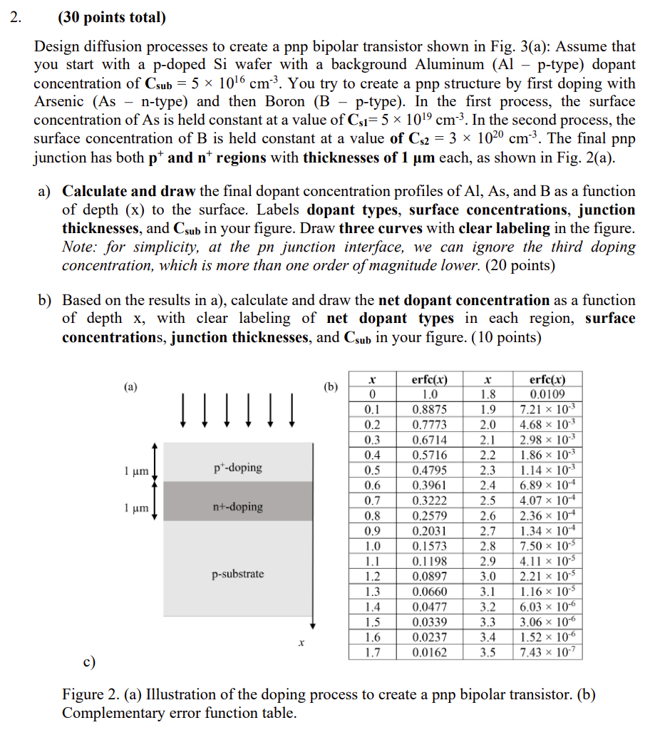
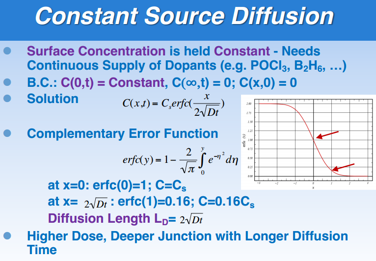
image text in transcribedimage text in transcribedimage text in transcribed
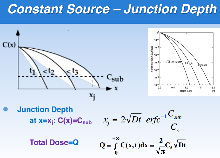
2. (30 points total) Design diffusion processes to create a pnp bipolar transistor shown in Fig. 3(a): Assume that you start with a p-doped Si wafer with a background Aluminum (Al - p-type) dopant concentration of Csub = 5 x 1016 cm . You try to create a pnp structure by first doping with Arsenic (As - n-type) and then Boron (B - p-type). In the first process, the surface concentration of As is held constant at a value of Csi=5 x 1019 cm-3. In the second process, the surface concentration of B is held constant at a value of Cs2 = 3 x 1020 cm. The final pnp junction has both p and n* regions with thicknesses of 1 um each, as shown in Fig. 2(a). a) Calculate and draw the final dopant concentration profiles of Al, As, and B as a function of depth (x) to the surface. Labels dopant types, surface concentrations, junction thicknesses, and Csub in your figure. Draw three curves with clear labeling in the figure. Note: for simplicity, at the pn junction interface, we can ignore the third doping concentration, which is more than one order of magnitude lower. (20 points) b) Based on the results in a), calculate and draw the net dopant concentration as a function of depth x, with clear labeling of net dopant types in each region, surface concentrations, junction thicknesses, and Csub in your figure. (10 points) (a) (b) X erfc(x) X erfc(x) 0 IIIIII 1.0 1.8 0.0109 01 0.8875 1.9 7.21 x 10⁻³ 0.2 0.7773 2.0 4.68 x 10⁻³ 0.3 0.6714 2.1 2.98 x 10⁻³ 0.4 0.5716 2.2 1.86 x 10⁻³ I um ] p*-doping 0.5 0.4795 2.3 1.14 x 10⁻³ 0.6 0.3961 2.4 6.89 x 10⁴ 1 um n+-doping 07 0.3222 2.5 4.07 x 10⁴ 0.8 0.2579 2.6 2.36 x 10⁴ 0.9 0.2031 2.7 1.34 x 10⁴ 1.0 0.1573 2.8 7.50 x 10⁻⁵ 0.1 198 2.9 4.11 x 10⁻⁵ p-substrate 1.2 0.0897 3.0 2.21 x 10⁻⁵ 1.3 0.0660 3.1 1.16 x 10⁻⁵ 1.4 0.0477 3.2 6.03 x 10⁻⁶ 1.5 0.0339 3.3 3.06 x 10-6 x 1.6 0.0237 3.4 1.52 x 10⁻⁶ C) 0.0162 3.5 7.43 x 10⁻⁷ Figure 2. (a) Illustration of the doping process to create a pnp bipolar transistor. (b) Complementary error function table.Constant Source Diffusion Surface Concentration is held Constant - Needs Continuous Supply of Dopants (e.g. POC13, B2H6, ...) B.C.: C(0,t) = Constant, C(oo,t) = 0; C(x,0) = 0 Solution C(x,t) = Cerfc( 21/ Dt Complementary Error Function 2 X erfc(y) = 1-- p-n dn at x=0: erfc(0)=1; C=CS at X= 2VDt : erfc(1)=0.16; C=0.16CS Diffusion Length LD= 2VDt Higher Dose, Deeper Junction with Longer Diffusion TimeConstant Source - Junction Depth 109 10-1 C(x) 10 10- Concentration/C (surface) 10-4- Voi = 0.15 um 0.2 um 0.25 um
Step by Step Solution

There are 3 Steps involved in it

Step: 1

blur-text-image

Get Instant Access to Expert-Tailored Solutions

See step-by-step solutions with expert insights and AI powered tools for academic success

Step: 2

blur-text-image

Step: 3

blur-text-image

Ace Your Homework with AI

Get the answers you need in no time with our AI-driven, step-by-step assistance

Get Started

Recommended Textbook for

Microoptics Technology Fabrication And Applications Of Lens Arrays And Devices

Authors: Nicholas F Borrelli

2nd Edition

1351836668, 9781351836661

More Books

Students also viewed these Physics questions

Question

What kinds of communication help sustain long-distance romances?

Answered: 1 week ago