Answered step by step
Verified Expert Solution
Question
1 Approved Answer
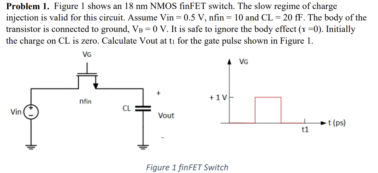
Figure 1 shows an 18 nm NMOS finFET switch. The slow regime ofcharge injection is valid for this circuit. Assume Vin = 0.5 V,nfin =
Figure 1 shows an 18 nm NMOS finFET switch. The slow regime ofcharge injection is valid for this circuit. Assume Vin = 0.5 V,nfin = 10 and CL = 20 fF. The body of the transistor is connectedto ground, VB = 0 V. It is safe to ignore the body effect (? =0).Initially the charge on CL is zero. Calculate Vout at t1 for thegate pulse shown in Figure 1.

Problem 1. Figure 1 shows an 18 nm NMOS finFET switch. The slow regime of charge injection is valid for this circuit. Assume Vin = 0.5 V, nfin = 10 and CL = 20 fF. The body of the transistor is connected to ground, V = 0 V. It is safe to ignore the body effect (x =0). Initially the charge on CL is zero. Calculate Vout at ti for the gate pulse shown in Figure 1. VG Vin nfin CL Vout +1 V Figure 1 finFET Switch VG t1 t (ps)
Step by Step Solution
★★★★★
3.49 Rating (159 Votes )
There are 3 Steps involved in it
Step: 1
Sol Given in the question Vin 05V nfin 10 GATE input pass t O 1 oo it ...
Get Instant Access to Expert-Tailored Solutions
See step-by-step solutions with expert insights and AI powered tools for academic success
Step: 2

Step: 3

Ace Your Homework with AI
Get the answers you need in no time with our AI-driven, step-by-step assistance
Get Started


