Answered step by step
Verified Expert Solution
Question
1 Approved Answer
Figure 3 shows the ANSI diagrams for a pair of Boolean gates known as NAND (not AND) and NOR (not OR). Those correspond to the
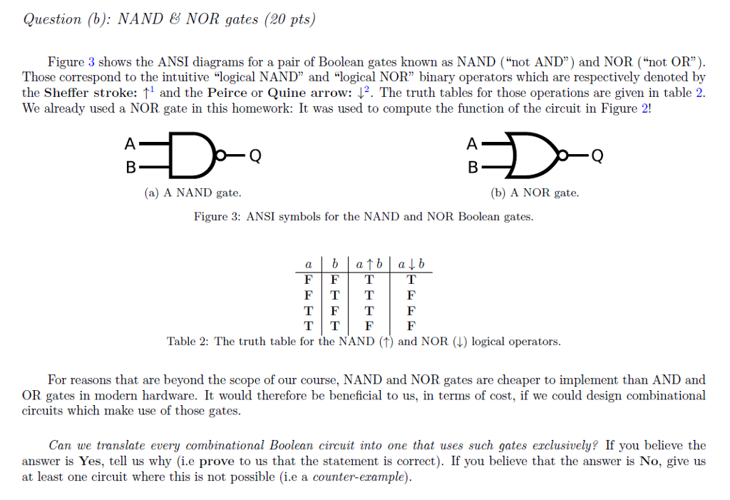
Figure 3 shows the ANSI diagrams for a pair of Boolean gates known as NAND ("not AND") and NOR ("not OR"). Those correspond to the intuitive "logical NAND" and "logical NOR" binary operators which are respectively denoted by the Sheffer stroke: uparrow^1 and the Peirce or Quine arrow: downarrow^2. The truth tables for those operations are given in table 2. We already used a NOR gate in this homework: It was used to compute the function of the circuit in Figure 2! For reasons that are beyond the scope of our course, NAND and NOR gates are cheaper to implement than AND and OR gates in modern hardware. It would therefore be beneficial to us, in terms of cost, if we could design combinational circuits which make use of those gates. Can we translate every combinational Boolean circuit into one that uses such gates exclusively? If you believe the answer is Yes, tell us why (i.e. prove to us that the statement is correct). If you believe that the answer is No, give us at least one circuit where this is not possible (i.e. a counter-example)
Step by Step Solution
There are 3 Steps involved in it
Step: 1
Get Instant Access to Expert-Tailored Solutions
See step-by-step solutions with expert insights and AI powered tools for academic success
Step: 2
Step: 3
Ace Your Homework with AI
Get the answers you need in no time with our AI-driven, step-by-step assistance
Get Started