

Question
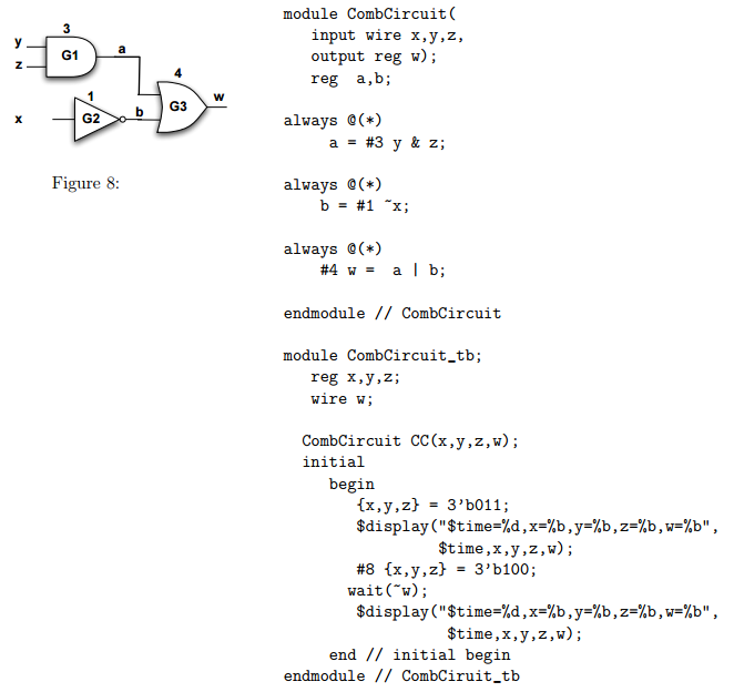
Figure 8 shows a simple combinational logic circuit. The numbers associated with each gate are the propagation delays. Below is a segment of Verilog behavioral
Figure 8 shows a simple combinational logic circuit. The numbers associated with each gate are the propagation delays. Below is a segment of Verilog behavioral code that describes the circuit, with a process (always blocks), corresponding to each gate.
{{{{module CombCircuit( input wire x,y,z, output reg w); reg a,b; always @(*) a = #3 y & z; always @(*) b = #1 ~x; always @(*) #4 w = a | b; endmodule // CombCircuit module CombCircuit_tb; reg x,y,z; wire w; CombCircuit CC(x,y,z,w); initial begin {x,y,z} = 3b011; $display("$time=%d,x=%b,y=%b,z=%b,w=%b", $time,x,y,z,w); #8 {x,y,z} = 3b100; wait(~w); $display("$time=%d,x=%b,y=%b,z=%b,w=%b", $time,x,y,z,w); end // initial begin endmodule // CombCiruit_tb }}}
(a) Write the ouput of a Verilog simulator would be after simulating the module CombCircuit tb.
(b) Does the Verilog module CombCircuit correctly model the propagation delay of the combinational logic in Figure 8? Explain your answer.
(c) If your answer to question (b) is negative, then identify what changes you would make and write the output of a Verilog simulator would be for the modified description.
Step by Step Solution
There are 3 Steps involved in it
Step: 1

Get Instant Access to Expert-Tailored Solutions
See step-by-step solutions with expert insights and AI powered tools for academic success
Step: 2

Step: 3
Ace Your Homework with AI
Get the answers you need in no time with our AI-driven, step-by-step assistance
Get Started
SQL Server Database Programming With Visual Basic.NET Concepts Designs And Implementations
Authors: Ying Bai
1st Edition
1119608503, 978-1119608509