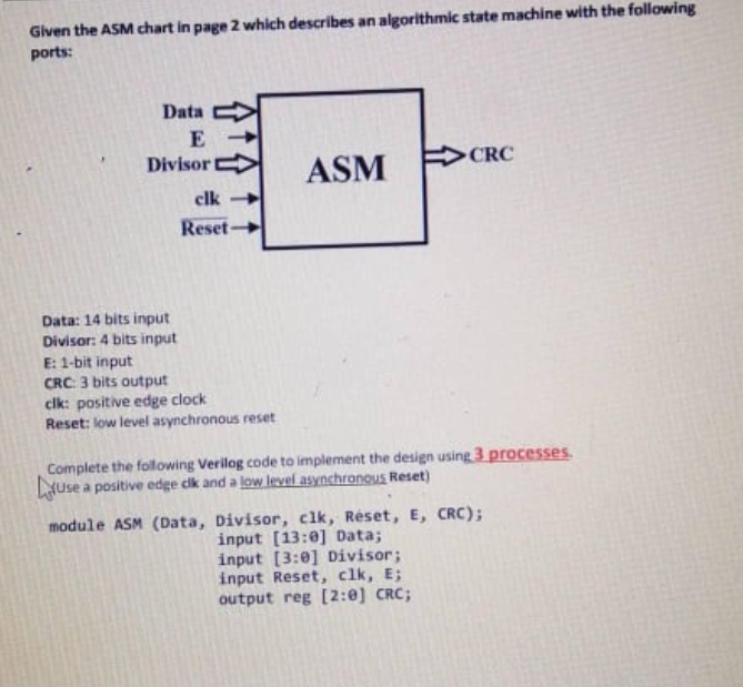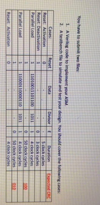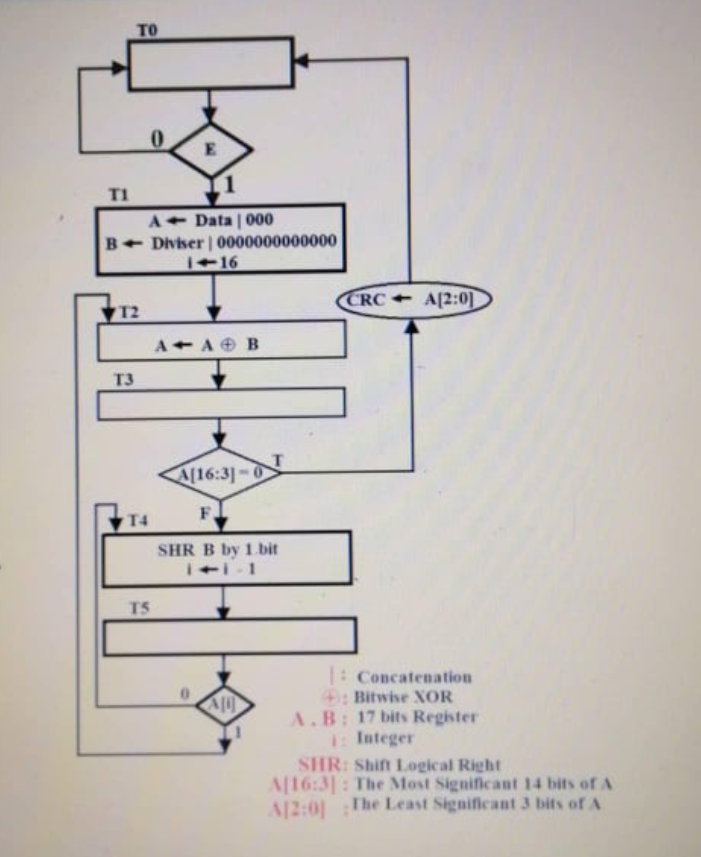


Given the ASM chart in page 2 which describes an algorithmic state machine with the following ports: CRC Data E Divisor cik Reset ASM Data: 14 bits input Divisor: 4 bits input E: 1-bit input CRC: 3 bits output clk: positive edge clock Reset: low level asynchronous reset Complete the following Verllog code to implement the design using 3 processes Luse a positive edge clk and a low level asynchronous Reset) module ASM (Data, Divisor, clk, Reset, E, CRC); input (13:0] Data; input (3:0) Divisor; input Reset, clk, E; output reg [2:) CRC; You have to submit two files: 1. A Verilog code to implement your ASM. 2. A testbench file to simulate and test your design. You should cover the following cases: Data Reset 0 Divisor Expected CRC Cases: Reset: Activation Reset: Deactivation Parallel Load Om 1 1 11010011101100 1011 Duration 5 clock cycles 3 clock cycles 4 clock cycles 50 clock cycles 4 clock cycles 50 clock cycles 4 clock cycles 1 100 Parallel Load 1 11000110000110 1011 0 1 0 010 Reset: Activation 0 TO 0 E TI A Data 1000 B+ Diviser 0000000000000 116 CRC = A[2:0) T2 A A AB T3 A[16:31 - F SHR B by 1 bit TS 10 1 : Concatenation Bitwise XOR 1.B : 17 bits Register Integer SHIR: Shin Logical Right A[16:31: The Most Significant 14 bits of 1/2:0 The Least Significant 3 bits of A Given the ASM chart in page 2 which describes an algorithmic state machine with the following ports: CRC Data E Divisor cik Reset ASM Data: 14 bits input Divisor: 4 bits input E: 1-bit input CRC: 3 bits output clk: positive edge clock Reset: low level asynchronous reset Complete the following Verllog code to implement the design using 3 processes Luse a positive edge clk and a low level asynchronous Reset) module ASM (Data, Divisor, clk, Reset, E, CRC); input (13:0] Data; input (3:0) Divisor; input Reset, clk, E; output reg [2:) CRC; You have to submit two files: 1. A Verilog code to implement your ASM. 2. A testbench file to simulate and test your design. You should cover the following cases: Data Reset 0 Divisor Expected CRC Cases: Reset: Activation Reset: Deactivation Parallel Load Om 1 1 11010011101100 1011 Duration 5 clock cycles 3 clock cycles 4 clock cycles 50 clock cycles 4 clock cycles 50 clock cycles 4 clock cycles 1 100 Parallel Load 1 11000110000110 1011 0 1 0 010 Reset: Activation 0 TO 0 E TI A Data 1000 B+ Diviser 0000000000000 116 CRC = A[2:0) T2 A A AB T3 A[16:31 - F SHR B by 1 bit TS 10 1 : Concatenation Bitwise XOR 1.B : 17 bits Register Integer SHIR: Shin Logical Right A[16:31: The Most Significant 14 bits of 1/2:0 The Least Significant 3 bits of A
