Answered step by step
Verified Expert Solution
Link Copied!

Question

1 Approved Answer

[H] CLO$: Analyze and design the biasing and the amplifier circuits of JFET Q8- Analyze the biasing and the amplifier circuits of JFET in the
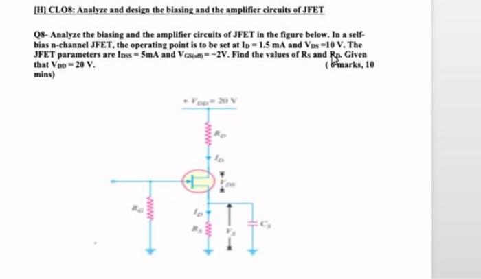
image text in transcribed
[H] CLO$: Analyze and design the biasing and the amplifier circuits of JFET Q8- Analyze the biasing and the amplifier circuits of JFET in the figure below. In a self- bias D-channel JFET, the operating point is to be set at lp - 1.5 mA and Vps -10 V. The JFET parameters are loss - 5mA and Vim-2V. Find the values of Rs and Rp. Given that Voo - 20 V. (marks, 10 mins)

Step by Step Solution

There are 3 Steps involved in it

Step: 1

blur-text-image

Get Instant Access to Expert-Tailored Solutions

See step-by-step solutions with expert insights and AI powered tools for academic success

Step: 2

blur-text-image_2

Step: 3

blur-text-image_3

Ace Your Homework with AI

Get the answers you need in no time with our AI-driven, step-by-step assistance

Get Started

Recommended Textbook for

Database And Transaction Processing

Authors: Philip M. Lewis, Arthur Bernstein, Michael Kifer

1st Edition

0201708728, 978-0201708721

More Books

Students also viewed these Databases questions