https://reference.digilentinc.com/textbooks:real_digital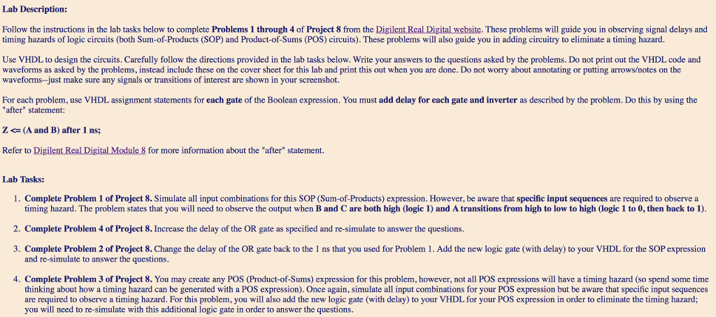
Follow the instructions in the lab tasks below to complete Problems 1 through 4 of Project 8 from the Digilent Real Digital website. These problems will guide you in observing signal delays and timing hazards of logic circuits (both Sum-of-Products (SOP) and Product-of-Sums (POS) circuits). These problems will also guide you in adding circuitry to eliminate a timing hazard. Use VHDL to design the circuits. Carefully follow the directions provided in the lab tasks below. Write your answers to the questions asked by the problems. Do not print out the VHDL code and waveforms as asked by the problems, instead include these on the cover sheet for this lab and print this out when you are done. Do not worry about annotating or putting arrowsotes on the waveforms-just make sure any signals or transitions of interest are shown in your screenshot. For each problem, use VHDL assignment statements for each gate of the Boolean expression. You must add delay for each gate and inverter as described by the problem. Do this by using the 'after" statement: Z (A and B) after 1 ns; Refer to Digilent Real Digital Module 8 for more information about the "after" statement. 1. Complete Problem 1 of Project 8. Simulate all input combinations for this SOP (Sum-of-Products) expression. However, be aware that specific input sequences are required to observe a timing hazard. The problem states that you will need to observe the output when B and C are both high (logic 1) and A transitions from high to low to high (logic 1 to 0, then back to 1). 2. Complete Problem 4 of Project 8. Increase the delay of the OR gate as specified and re-simulate to answer the questions. 3. Complete Problem 2 of Project 8. Change the delay of the OR gate back to the 1 ns that you used for Problem 1. Add the new logic gate (with delay) to your VHDL for the SOP expression and re-simulate to answer the questions. 4. Complete Problem 3 of Project 8. You may create any POS (Product-of-Sums) expression for this problem, however, not all POS expressions will have a timing hazard (so spend some time thinking about how a timing hazard can be generated with a POS expression). Once again, simulate all input combinations for your POS expression but be aware that specific input sequences are required to observe a timing hazard. For this problem, you will also add the new logic gate (with delay) to your VHDL for your POS expression in order to eliminate the timing hazard; you will need to re-simulate with this additional logic gate in order to answer the questions. Follow the instructions in the lab tasks below to complete Problems 1 through 4 of Project 8 from the Digilent Real Digital website. These problems will guide you in observing signal delays and timing hazards of logic circuits (both Sum-of-Products (SOP) and Product-of-Sums (POS) circuits). These problems will also guide you in adding circuitry to eliminate a timing hazard. Use VHDL to design the circuits. Carefully follow the directions provided in the lab tasks below. Write your answers to the questions asked by the problems. Do not print out the VHDL code and waveforms as asked by the problems, instead include these on the cover sheet for this lab and print this out when you are done. Do not worry about annotating or putting arrowsotes on the waveforms-just make sure any signals or transitions of interest are shown in your screenshot. For each problem, use VHDL assignment statements for each gate of the Boolean expression. You must add delay for each gate and inverter as described by the problem. Do this by using the 'after" statement: Z (A and B) after 1 ns; Refer to Digilent Real Digital Module 8 for more information about the "after" statement. 1. Complete Problem 1 of Project 8. Simulate all input combinations for this SOP (Sum-of-Products) expression. However, be aware that specific input sequences are required to observe a timing hazard. The problem states that you will need to observe the output when B and C are both high (logic 1) and A transitions from high to low to high (logic 1 to 0, then back to 1). 2. Complete Problem 4 of Project 8. Increase the delay of the OR gate as specified and re-simulate to answer the questions. 3. Complete Problem 2 of Project 8. Change the delay of the OR gate back to the 1 ns that you used for Problem 1. Add the new logic gate (with delay) to your VHDL for the SOP expression and re-simulate to answer the questions. 4. Complete Problem 3 of Project 8. You may create any POS (Product-of-Sums) expression for this problem, however, not all POS expressions will have a timing hazard (so spend some time thinking about how a timing hazard can be generated with a POS expression). Once again, simulate all input combinations for your POS expression but be aware that specific input sequences are required to observe a timing hazard. For this problem, you will also add the new logic gate (with delay) to your VHDL for your POS expression in order to eliminate the timing hazard; you will need to re-simulate with this additional logic gate in order to answer the questions