I know this is a lot, but if I could get some sort of guidance.
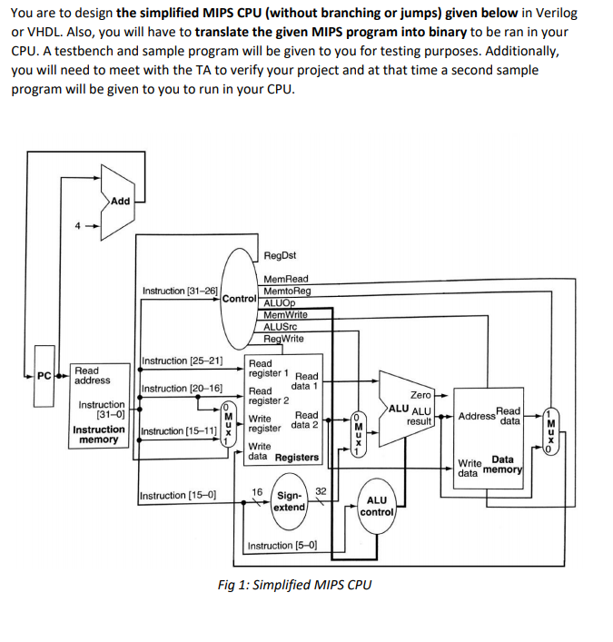
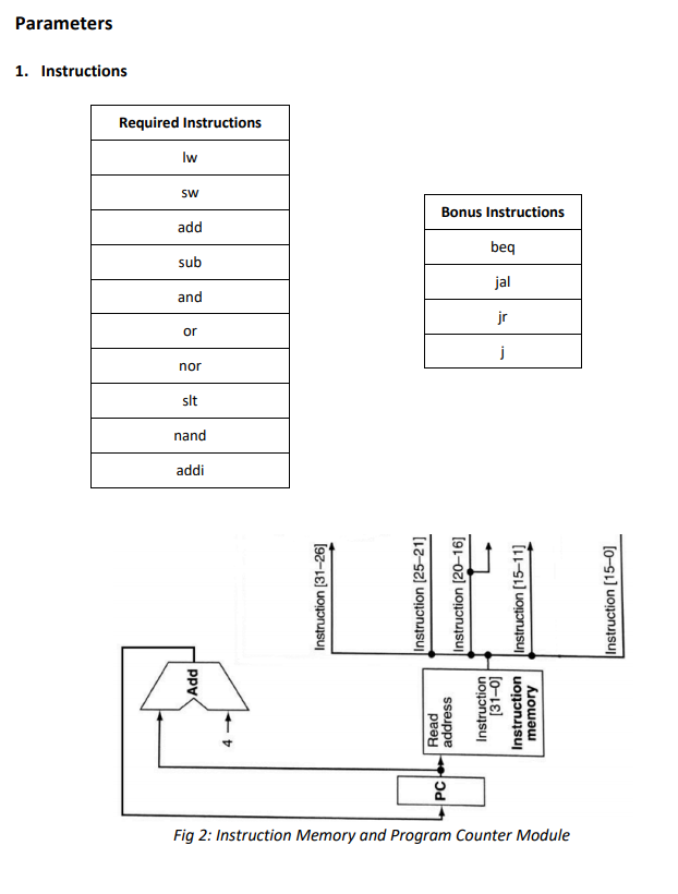
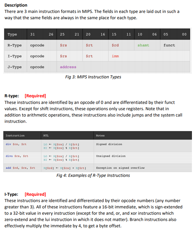
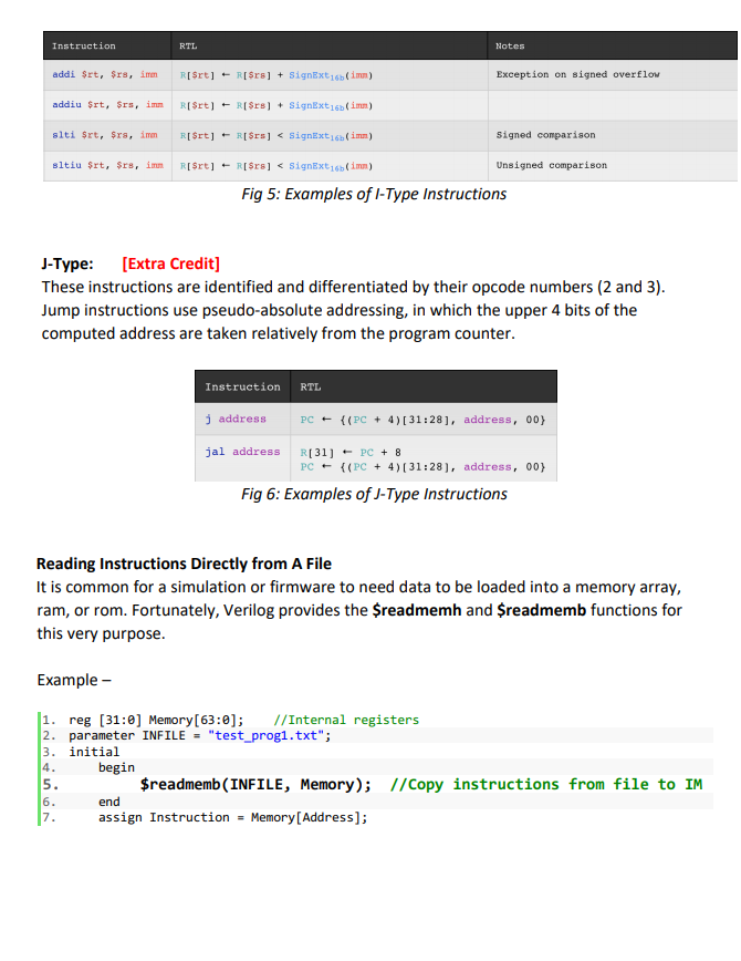
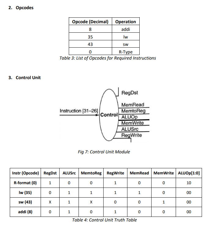
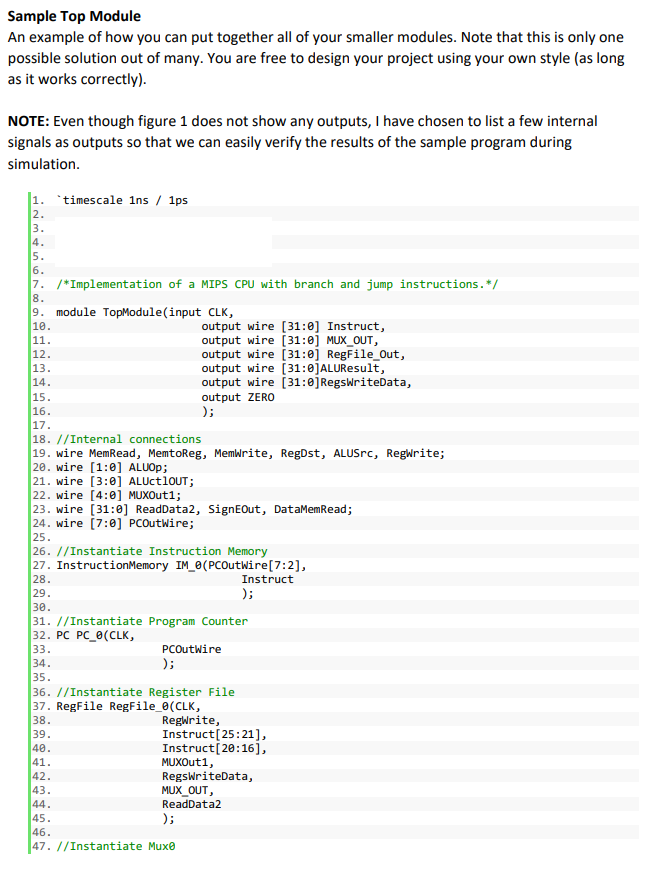
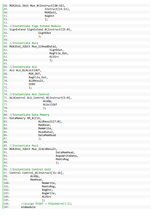
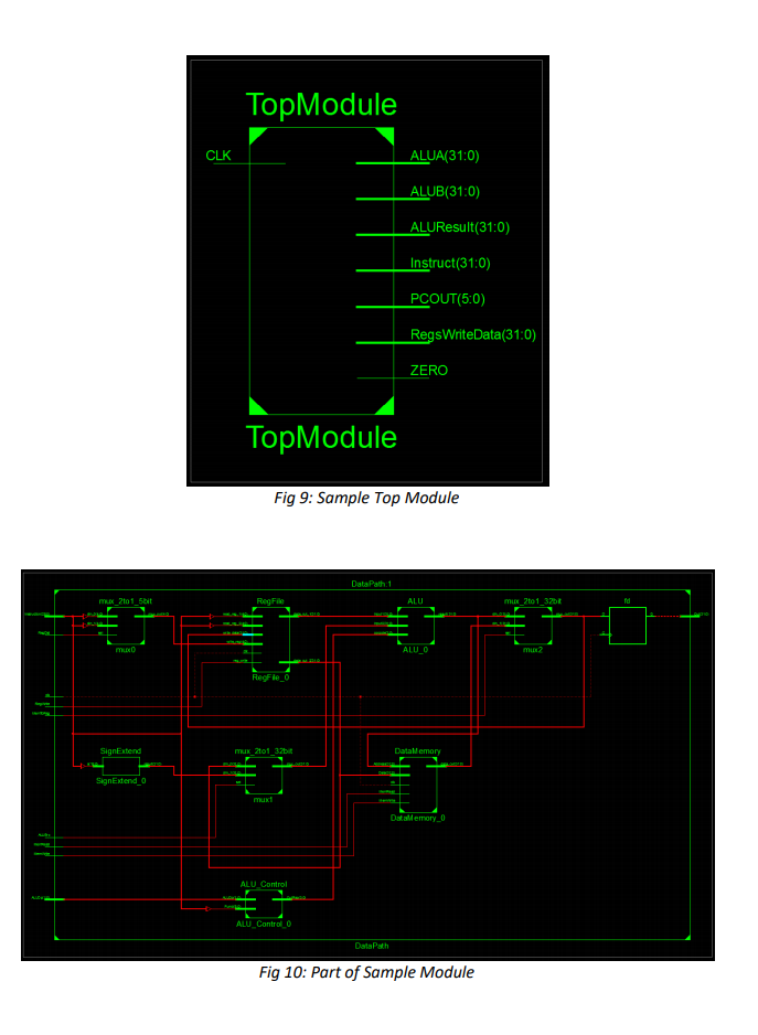
You are to design the simplified MIPS CPU (without branching or jumps) given below in Verilog or VHDL. Also, you will have to translate the given MIPS program into binary to be ran in your CPU. A testbench and sample program will be given to you for testing purposes. Additionally you will need to meet with the TA to verify your project and at that time a second sample program will be given to you to run in your CPU Add MemRead Instruction (31-261 Control ALL Instruction [25-21 Read register 1 Read data 1 1 PC Read Instruction [20-16 Read Zero ALU ALU result register 2 [31-0 Instruction Instruction (15regi Write Read [15-11]register data 2 Read Address data data Registers Write Data data 16 Sign- extend Instruction [15-0] ALU control Instruction (5-0) Fig 1: Simplified MIPS CPU For the given function you will need to write the MIPS code and translate that into binary (follow the example that is given in the test program). You can't use multiply or shift, and you can either load g and h into data memory or use the add immediate instruction (addi). You will need to turn in a asm file with the code and a.txt file with the binary Equation 1: Given function Extra Credit (5 points): Implement branching and jumps Submission You will only need to complete a lab report, following the ECE Style Guide. In the results section you will need the following: 1. Waveforms 2. Synthesized RTL schematic Also, you will need to turn in any Verilog or VHDL files associated with the lab. Parameters 1. Instructions Required Instructions lw SW add sub and Bonus Instructions beq jal or nor nand addi Fig 2: Instruction Memory and Program Counter Module Description There are 3 main instruction formats in MIPS. The fields in each type are laid out in sucha way that the same fields are always in the same place for each type 26 25 21 20 11 10 06 05 Type R-Type opcode I-Type opcode J-Type opcode 31 16 15 rs Srt Srd shamt funct rs rt imm address Fig 3: MIPS Instruction Types R-type: [Required] These instructions are identified by an opcode of 0 and are differentiated by their funct values. Except for shift instructions, these operations only use registers. Note that in addition to arithmetic operations, these instructions also include jumps and the system call instruction Instruction RTL Notes div Srs, Srt signed division divu $rs, rt Unsigned division add Srd, Srs, $rt Exception on signed overflow Fig 4: Examples of R-Type Instructions I-Type: [Required] These instructions are identified and differentiated by their opcode numbers (any number greater than 3). All of these instructions feature a 16-bit immediate, which is sign-extended to a 32-bit value in every instruction (except for the and, or, and xor instructions which zero-extend and the lui instruction in which it does not matter). Branch instructions also effectively multiply the immediate by 4, to get a byte offset. Instruction RTL Notes Exception on signed overflow Signed comparison Unsigned comparison Fig 5: Examples of I-Type Instructions J-Type: [Extra Credit] These instructions are identified and differentiated by their opcode numbers (2 and 3) Jump instructions use pseudo-absolute addressing, in which the upper 4 bits of the computed address are taken relatively from the program counter Instruct i n RTL j address PC (PC + 4)[ 31:28], address, 00) jal address R[31PC8 PC (PC + 4) 31:28], address, 00) Fig 6: Examples of J-Type Instructions Reading Instructions Directly from A File It is common for a simulation or firmware to need data to be loaded into a memory array, ram, or rom. Fortunately, Verilog provides the readmemh and readmemb functions for this very purpose Example 1. reg [31:0] Memory [63:0]; //Internal registers 2. parameter INFILE"test prog1.txt" 3. initial 4 5 6 begin $readmemb (INFILE, Memory) //Copy instructions from file to IM end assign Instruction -Memory[Address]; 2. Opcodes Opcode (Decimal) Operation addi lw SW R-Type 35 0 Table 3: List of Opcodes for Required Instructions 3. Control Unit RegDst MemRead MemtoRe Instruction [31-26] Control ALUOP MemWrite ALUSrc RegWrite Fig 7: Control Unit Module Instr (Opcode) RegDstALUSrc MemtoReg RegWrite MemRead MemWrite ALUOp[1:0] R-format (0 1 lw (35) sw (43) addi (8) 1 10 1 1 1 Table 4: Control Unit Truth Table 48. MUX2tol_5bit Mux_e(Instruct[20:16], 49 50 51. 52 53 54. //Instantiate Sign Extend Module 55. SignExtend SignExtend 0 (Instruct[ 15:01, 56 57. 58 59. //Instantiate Mux1 60. MUX2to132bit Mux_1(ReadData2, 61. 62 63 64 65. 66. //Instantiate ALU 67. ALU ALU 0 (ALUctlOUT, 68 69 70 Instruct[15:11], MUXOut1, RegDst SignEOut SignEOut, RegFile_Out, ALUSrc MUX OUT RegFile Out, ALUResult, ZERO 72. 73 74. //Instantiate ALU Control 75. ALUControl ALU Control (Instruct [5:01, 76 ALUOp, ALUctloUT 78 79 80. //Instantiate Data Memory 81. DataMemory DM 0 (CLK, 82. 83 84. 85 86 87. ALUResult[7:0] MemRead, Memwrite, ReadData2, DataMemRead 89. //Instantiate Mux2 90. MUX2to132bit Mux_2 (ALUResult, 91 92. 93 94. 95 96. //Instantiate Control Unit 97. Control Control_8(Instruct[31:26], 98 DataMemRead, RegswriteData, MemtoReg ALUOp, MemRead, 100 101 102 103 104 105 106 107. Memwrite, MemtoReg, RegDst, Regwrite, ALUSrc //assign PCOUT-PCOutwire[7:2]; endmodule TopModule CLK ALUA(31:0) ALUB(31:0) ALUResult(31:0) Instruct(31:0) PCOUT(5:0) RegsWriteData(31:0 ZERO TopModule Fig 9: Sample Top Module mx 2t01_5bit RegFile ALU mux 2to1_32 MLxO ALU mux2 DstalMemory ALU Control LU Control Fig 10: Part of Sample Module You are to design the simplified MIPS CPU (without branching or jumps) given below in Verilog or VHDL. Also, you will have to translate the given MIPS program into binary to be ran in your CPU. A testbench and sample program will be given to you for testing purposes. Additionally you will need to meet with the TA to verify your project and at that time a second sample program will be given to you to run in your CPU Add MemRead Instruction (31-261 Control ALL Instruction [25-21 Read register 1 Read data 1 1 PC Read Instruction [20-16 Read Zero ALU ALU result register 2 [31-0 Instruction Instruction (15regi Write Read [15-11]register data 2 Read Address data data Registers Write Data data 16 Sign- extend Instruction [15-0] ALU control Instruction (5-0) Fig 1: Simplified MIPS CPU For the given function you will need to write the MIPS code and translate that into binary (follow the example that is given in the test program). You can't use multiply or shift, and you can either load g and h into data memory or use the add immediate instruction (addi). You will need to turn in a asm file with the code and a.txt file with the binary Equation 1: Given function Extra Credit (5 points): Implement branching and jumps Submission You will only need to complete a lab report, following the ECE Style Guide. In the results section you will need the following: 1. Waveforms 2. Synthesized RTL schematic Also, you will need to turn in any Verilog or VHDL files associated with the lab. Parameters 1. Instructions Required Instructions lw SW add sub and Bonus Instructions beq jal or nor nand addi Fig 2: Instruction Memory and Program Counter Module Description There are 3 main instruction formats in MIPS. The fields in each type are laid out in sucha way that the same fields are always in the same place for each type 26 25 21 20 11 10 06 05 Type R-Type opcode I-Type opcode J-Type opcode 31 16 15 rs Srt Srd shamt funct rs rt imm address Fig 3: MIPS Instruction Types R-type: [Required] These instructions are identified by an opcode of 0 and are differentiated by their funct values. Except for shift instructions, these operations only use registers. Note that in addition to arithmetic operations, these instructions also include jumps and the system call instruction Instruction RTL Notes div Srs, Srt signed division divu $rs, rt Unsigned division add Srd, Srs, $rt Exception on signed overflow Fig 4: Examples of R-Type Instructions I-Type: [Required] These instructions are identified and differentiated by their opcode numbers (any number greater than 3). All of these instructions feature a 16-bit immediate, which is sign-extended to a 32-bit value in every instruction (except for the and, or, and xor instructions which zero-extend and the lui instruction in which it does not matter). Branch instructions also effectively multiply the immediate by 4, to get a byte offset. Instruction RTL Notes Exception on signed overflow Signed comparison Unsigned comparison Fig 5: Examples of I-Type Instructions J-Type: [Extra Credit] These instructions are identified and differentiated by their opcode numbers (2 and 3) Jump instructions use pseudo-absolute addressing, in which the upper 4 bits of the computed address are taken relatively from the program counter Instruct i n RTL j address PC (PC + 4)[ 31:28], address, 00) jal address R[31PC8 PC (PC + 4) 31:28], address, 00) Fig 6: Examples of J-Type Instructions Reading Instructions Directly from A File It is common for a simulation or firmware to need data to be loaded into a memory array, ram, or rom. Fortunately, Verilog provides the readmemh and readmemb functions for this very purpose Example 1. reg [31:0] Memory [63:0]; //Internal registers 2. parameter INFILE"test prog1.txt" 3. initial 4 5 6 begin $readmemb (INFILE, Memory) //Copy instructions from file to IM end assign Instruction -Memory[Address]; 2. Opcodes Opcode (Decimal) Operation addi lw SW R-Type 35 0 Table 3: List of Opcodes for Required Instructions 3. Control Unit RegDst MemRead MemtoRe Instruction [31-26] Control ALUOP MemWrite ALUSrc RegWrite Fig 7: Control Unit Module Instr (Opcode) RegDstALUSrc MemtoReg RegWrite MemRead MemWrite ALUOp[1:0] R-format (0 1 lw (35) sw (43) addi (8) 1 10 1 1 1 Table 4: Control Unit Truth Table 48. MUX2tol_5bit Mux_e(Instruct[20:16], 49 50 51. 52 53 54. //Instantiate Sign Extend Module 55. SignExtend SignExtend 0 (Instruct[ 15:01, 56 57. 58 59. //Instantiate Mux1 60. MUX2to132bit Mux_1(ReadData2, 61. 62 63 64 65. 66. //Instantiate ALU 67. ALU ALU 0 (ALUctlOUT, 68 69 70 Instruct[15:11], MUXOut1, RegDst SignEOut SignEOut, RegFile_Out, ALUSrc MUX OUT RegFile Out, ALUResult, ZERO 72. 73 74. //Instantiate ALU Control 75. ALUControl ALU Control (Instruct [5:01, 76 ALUOp, ALUctloUT 78 79 80. //Instantiate Data Memory 81. DataMemory DM 0 (CLK, 82. 83 84. 85 86 87. ALUResult[7:0] MemRead, Memwrite, ReadData2, DataMemRead 89. //Instantiate Mux2 90. MUX2to132bit Mux_2 (ALUResult, 91 92. 93 94. 95 96. //Instantiate Control Unit 97. Control Control_8(Instruct[31:26], 98 DataMemRead, RegswriteData, MemtoReg ALUOp, MemRead, 100 101 102 103 104 105 106 107. Memwrite, MemtoReg, RegDst, Regwrite, ALUSrc //assign PCOUT-PCOutwire[7:2]; endmodule TopModule CLK ALUA(31:0) ALUB(31:0) ALUResult(31:0) Instruct(31:0) PCOUT(5:0) RegsWriteData(31:0 ZERO TopModule Fig 9: Sample Top Module mx 2t01_5bit RegFile ALU mux 2to1_32 MLxO ALU mux2 DstalMemory ALU Control LU Control Fig 10: Part of Sample Module