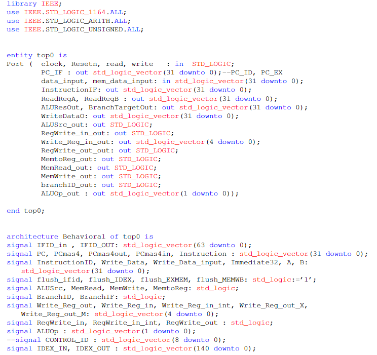
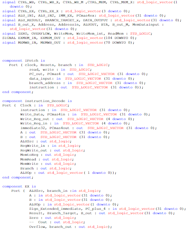
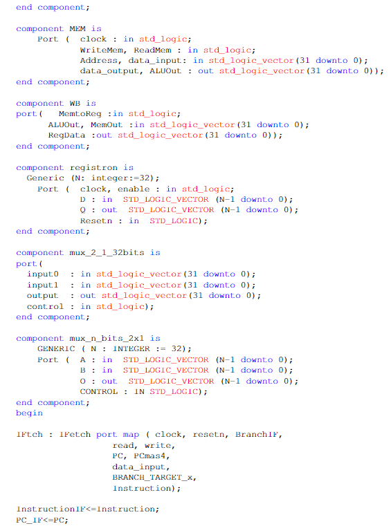
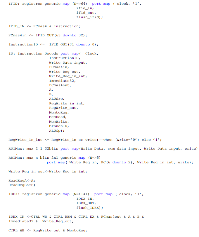
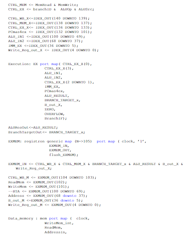
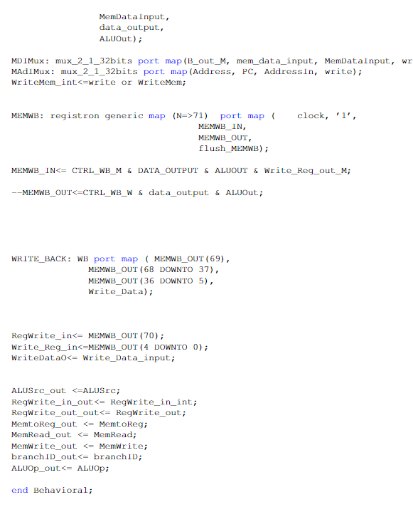
I need a testbench code to run the simulation of this program in Vivado (VHDL)below.
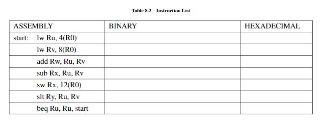
Prepare a TEST BENCH file issuing the instructions in table 8.2 to the DATA INPUT port signal, while setting the WRITE input. The WRITE input also enables to write data into the Data Memory and Registers. The data to be written to both must be issued through the MEM_DATA_INPUT input, while the address is issued by the PC to the Data Memory and the register number is issued by PC(6 downto 2) to the Register File. At the same time that you are writing the instructions, write any data easy to recognize to the Register File and Data Memory. Remember the RESETN signal must be low at the beginning of the instruction/data writing, and must be low again at the beginning of the execution.


Table 8.2 Instruction List ASSEMBLY BINARY HEXADECIMAL start: w Ru, 4(R0) lw Rv, 8(RO) add Rw, Ru, Rv sub Rx, Ru. Rv sw Rx, 12(RO) slt Ry, Ru, Rv beq Ru, Ru, start library IEEE use IEEE.STD_LOGIC_1164.ALL; use IEEE. STD_LOGIC_ARITH.ALL use IEEE. STD_LOGIC_UNSIGNED.ALL; entity top0 is Port clock, Resetn, read, write :in STD_LOGIC; PC_IF : out std logic_vector (31 downto 0)PC_ID, PC_EX data input, mem_data_input: in std logic_vector (31 downto 0) InstrutionIF: out std_logic_vector (31 downto 0) ReadRegA, ReadRegBout std logic_vector (31 downto 0) ALUResOut, BranchTargetOut: out std logic_vector (31 downto 0) WriteDataO: out std_logic_vector (31 downto 0) ALUSrc_out: out STD_ LOGIC; RegWrite_in_out: out STD_LOGIC Write_Reg in_ out: out std_logic_vector (4 downto 0) RegWrite_out_out: out STD_LOGIC; MemtoReg_out: out STD_LOGIC; MemRead_out: out STD_LOGIC; MemWrite_out: out STD_LOGIC branchID out out STD LOGIC: ALUOp_out out stdlogic_vector (1 downto 0)) end topo; architecture Behavioral of top0 is signal IFID_in, IFID_OUT: std_logic_vector (63 downto 0) signal PC, PCmas4, PCmas4out, PCmas4in, Instruction std logic_vector (31 downto 0); signal InstructionID, Write_Data, Write_Data_input, Immediate32, A, B: std logic_vector (31 downto 0) signal flushifid, flush_IDEX, flush_EXMEM, flush_MEMWB: std logic:-'1 signal ALUSrc, MemRead, MemWrite, MemtoReg: std_logic; signal BranchID, BranchIF: std_logic; signal Write_Reg out, Write_ Reg_in, Write_Reg_in_int, Write_Reg_out_X, Write_Reg_out_M: stdlogic_vector (4 downto 0); signal RegWrite_in, RegWrite_in_int, Regwrite_out: std logic; signal ALUOp : std_logic_vector (1 downto 0) signal CONTROL_ID:std_ logic_vector (8 downto 0) signal IDEX_IN, IDEX_OUT: std_logic_vector (140 downto 0); signal CTRL_ W, CTRL WBX, CTRL _WBM ,CTRL_MEM, CTRL_MEM X: std logic_vector (1 downto 0) signal CTRL EX, CTRL EXX: std logic_vector (3 downto 0) signal ALU IN1, ALU_IN2, IMM EX, PCmas4ex: std logic_vector (31 downto 0) signal ALU_ RESULT, BRANCH_TARGETx, DATA OUTPUT stdlogic vector (31 downto 0) signal B_out_X, Address, AddressIn, ALUOUT, BTA, B out_M, MemDatainput: std logic vector (31 downto 0) signal ZERO, OVERELOW, WriteMem, WriteMem_int, ReadMem STD_LOGIC SIGNAL EXMEM IN, EXMEM OUT std logic_vector (104 DOWNTO 0) signal MEMWB IN, MEMWB_OUT : stdlogic_ vector (70 DOWNTO 0) component IF'et.ch is Port clock, Resetn, branch in STD LOGIC read, write : in STD LOGIC; PC_out, PCmas4ot STD LOGIC VECTOR (31 downto 0) data input: in STD_LOGIC VECTOR (31 downt.o 0) branch address in STD_LOGICVECTOR (31 downto 0) Instruction:out STD LOGIC VECTOR (31 downto 0)) end component component Instruction Decode is Port Clock:in STD LOGIC instruction : in STD-LOGIC VECTOR (31 downto 0); Write_Data, PCmas4in : in SIDLOGIC_VECTOR (31 downto 0) Write Reg-out : out STD-LOGIC VECTOR (4 downto 0); Write_ Reg_in in STD LOGIC VECTOR (4 downto 0) Immediate32, PCmas4out: out STD LOGIC_VECTOR (31 downto 0); A: out STD LOGIC_VECTOR (31 downto 0) B out STD LOGIC_VECTOR (31 downto 0) ALUSrc : out std logic; Regwritein : in std logic; Regwrite out: out std logic; MemtoReg out std logic; MemRead out std_logic; Memwrite:out std logic; Branch: out std_logic; ALUOp out std logic_vect.or 1 downto 0)) end component. component EX is Port ALUSc, branch_in :in std logic; A:in std_logic vector (31 downt.o 0) B: in st.d logic vector (31 downt.o 0) ALUOp : in std logic vector (1 downto 0) Sign Extended Immediate, PC plus_4 in std_logic_vector (31 downt.o 0) Result,Branch_Target, B out: out std logic vector (31 downt.o 0) Zero out std logic; Cout out stdlogic; Ovrflow, branch out out std_logic); end component component MEM is Port clock in std logic WriteMem, ReadMem in std logic; Address, data input: in std_ logic vect.or (31 downto 0) data output, ALUOut : out std logic vect.or (31 downto 0)) end component component WB is portMemtoReg in std_logic; ALUOut, MemOut in std logic_vector (31 downto 0) RegData :out std_logic vect.or (31 downto 0)) end component component registron is Generic (N: integer:-32) Port clock, enable in std_logic; D:in STD LOGIC VECTOR (N-1 downto 0) Q : out STD-LOGIC-VECTOR (N-1 downto 0); Resetn : in STD_LOGIC) end component component mux 2_1_32bits is port( inputo:in std logic vector (31 downt.o 0) input: in std logic vector (31 downt.o 0) output out std_logic vector (31 downto 0) cont.rol : in std logic) end component component mux n bits 2x1 is GENERIC N INTEGER 32) Port A:in STD LOGIC VECTOR (N-1 downto 0) B in STD LOGIC VECTOR (N-1 downto 0) : out STD_LOGIC_VECTOR (N-1 downto 0); CONTROLIN STD LOGIC) end component begin IFtch: IFetch port map clock, resetn, BranchlF, read, write, PC, PCmas4, data_input, BRANCH TARGET X, Instruction) InstructionIE PC_1F64) port map ( clock, , 1', ifid in, ifid out, flush ifid); IELD-IN 5) port map Write_ Reg in, PC (6 downto 2), Write_ Req_in int, write); write-Reg-in out. 141) port map clock, '1', IDEX IN, IDEX OUT, flush_IDEX) IDEXIN 71) port map ( clock, 1 MEMWBIN, MEMWB OUT, flush MEMWB MEIMWB_LN64) port map ( clock, , 1', ifid in, ifid out, flush ifid); IELD-IN 5) port map Write_ Reg in, PC (6 downto 2), Write_ Req_in int, write); write-Reg-in out. 141) port map clock, '1', IDEX IN, IDEX OUT, flush_IDEX) IDEXIN 71) port map ( clock, 1 MEMWBIN, MEMWB OUT, flush MEMWB MEIMWB_LN
