

Answered step by step
Verified Expert Solution
Question
1 Approved Answer
I need some help on this question! thank you ! REVIEW QUESTIONS 4 Data is transferred from Memory Tx to Memory Rx starting from the
 I need some help on this question! thank you !
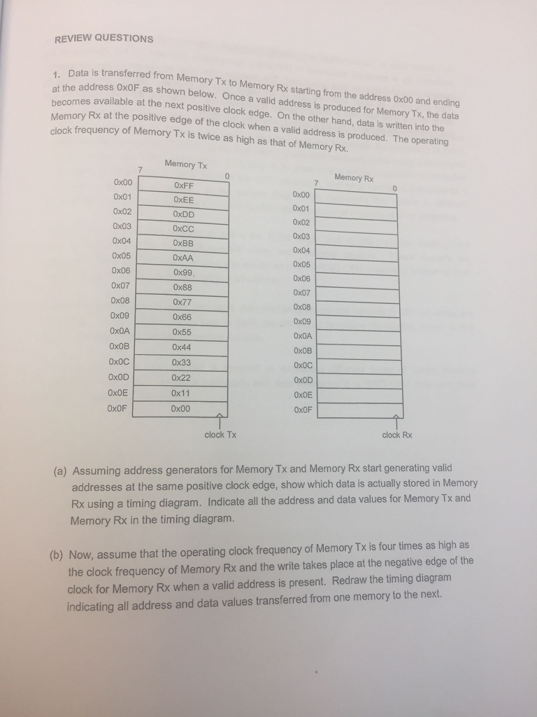
REVIEW QUESTIONS 4 Data is transferred from Memory Tx to Memory Rx starting from the address 0x00 and ending at the address 0xOF as shown below. Once a valld address is produced for Memory Tx, the data s available at the next positive clock edge. On the other hand, data is written into the ory Rx at the positive edge of the clock when a valid address is produced. The operating k frequency of Memory Tx is twice as high as that of Memory Rx. Memory T>x 0xFF OxEE 0xDD OxCC 0xBB OxAA 0x99 0x88 0x77 0x66 0x55 0x44 0x33 0x22 0x11 0x00 Memory Rx 0x00 0x01 0x02 0x03 0x04 0x05 0x06 0x07 0x08 0x09 0x01 0x03 0x04 0x05 0x06 0x08 0x09 0x0A 0x0B OxOB 0x0C 0xOD 0xOE OxOF 0x0D 0X0E 0xOF clock Tx clock Rx (a) Assuming address generators for Memory Tx and Memory Rx start generating valid addresses at the same positive clock edge, show which data is actually stored in Memory Rx using a timing diagram. Indicate all the address and data values for Memory Tx and Memory Rx in the timing diagram. (b) Now, assume that the operating clock frequency of Memory Tx is four times as high as the clock frequency of Memory Rx and the write takes place at the negative edge of the clock for Memory Rx when a valid address is present. Redraw the timing diagram indicating all address and data values transferred from one memory to the next REVIEW QUESTIONS 4 Data is transferred from Memory Tx to Memory Rx starting from the address 0x00 and ending at the address 0xOF as shown below. Once a valld address is produced for Memory Tx, the data s available at the next positive clock edge. On the other hand, data is written into the ory Rx at the positive edge of the clock when a valid address is produced. The operating k frequency of Memory Tx is twice as high as that of Memory Rx. Memory T>x 0xFF OxEE 0xDD OxCC 0xBB OxAA 0x99 0x88 0x77 0x66 0x55 0x44 0x33 0x22 0x11 0x00 Memory Rx 0x00 0x01 0x02 0x03 0x04 0x05 0x06 0x07 0x08 0x09 0x01 0x03 0x04 0x05 0x06 0x08 0x09 0x0A 0x0B OxOB 0x0C 0xOD 0xOE OxOF 0x0D 0X0E 0xOF clock Tx clock Rx (a) Assuming address generators for Memory Tx and Memory Rx start generating valid addresses at the same positive clock edge, show which data is actually stored in Memory Rx using a timing diagram. Indicate all the address and data values for Memory Tx and Memory Rx in the timing diagram. (b) Now, assume that the operating clock frequency of Memory Tx is four times as high as the clock frequency of Memory Rx and the write takes place at the negative edge of the clock for Memory Rx when a valid address is present. Redraw the timing diagram indicating all address and data values transferred from one memory to the next
Step by Step Solution
There are 3 Steps involved in it
Step: 1

Get Instant Access to Expert-Tailored Solutions
See step-by-step solutions with expert insights and AI powered tools for academic success
Step: 2

Step: 3
Ace Your Homework with AI
Get the answers you need in no time with our AI-driven, step-by-step assistance
Get Started
Introduction To Database And Knowledge Base Systems
Authors: S Krishna
1st Edition
9810206208, 978-9810206208