

Question
I would be happy if you can kindly help me . I've tried several times to solve this, but I couldn't.maybe the question might seem
I would be happy if you can kindly help me . I've tried several times to solve this, but I couldn't.maybe the question might seem long, but it is not, because I've attached all the files to make it clear. Please, I just need to compile all the components for the given operation as shown in the attachments. Your assistance would mean a lot to me
i dont need the simulation, just compile the components
thanks for your help and your time
single cycle using the component (control_unit, DataMemory, func_unit, Mux2x1_16bit, reg)
already defined all the components in another window or set of files using Quartus in my laptop
library ieee; use IEEE.STD_LOGIC_1164.ALL; use IEEE.STD_LOGIC_ARITH.ALL; use IEEE.STD_LOGIC_UNSIGNED.ALL;
entity control_unit is port( clk : in STD_LOGIC; V,C,N,Z : in std_logic; zerofill_out: out std_logic_vector(15 downto 0); a_in: in std_logic_vector(15 downto 0); da_out, ba_out, aa_out : out std_logic_vector(2 downto 0); mb_out, md_out, rw_out, mw_out: out std_logic; fs_out: out std_logic_vector(3 downto 0) ); end control_unit;
architecture Behavioral of control_unit is
signal count,AD : std_logic_vector(5 downto 0):="000000"; signal pl,jb,bc : std_logic;
-- ROM definition; Since count is 6 bits, the ROM capacity is 64 rows. type rom_type is array (0 to 63) of std_logic_vector (15 downto 0);
signal rom : rom_type := ( others => "0000000000000000" );
signal instruction : std_logic_vector(15 downto 0);
begin -- Codes for operations to be performed: example; rom(0)
-- Program counter operations pc: process (clk) begin if rising_edge(clk) then if pl = '0' then count
-- ROM operations instruction
-- Decoder operations da_out
-- Zerofill operation zerofill_out
-- Extend operation AD
end Behavioral;
library IEEE; use IEEE.STD_LOGIC_1164.ALL; use IEEE.STD_LOGIC_ARITH.ALL; use IEEE.STD_LOGIC_UNSIGNED.ALL;
entity DataMemory is Port ( MW : in STD_LOGIC; Data_in : in STD_LOGIC_VECTOR (15 downto 0); Address : in STD_LOGIC_VECTOR (15 downto 0); Data_out : out STD_LOGIC_VECTOR (15 downto 0); clk : in std_LOGIC); end DataMemory;
architecture Behavioral of DataMemory is
type mem_type is array (0 to 255) of std_logic_vector (15 downto 0); signal mem_cells: mem_type;
begin
process (clk) begin if (rising_edge(clk)) then if (MW = '1') then mem_cells(conv_integer(Address(7 downto 0)))
end Behavioral;
library IEEE; use IEEE.STD_LOGIC_1164.ALL; use IEEE.STD_LOGIC_ARITH.ALL; use IEEE.STD_LOGIC_UNSIGNED.ALL;
----------------------------------------------- -- A register file consisting of 8 registers, each 16 bits. -- The register file operates as a clock-independent RAM structure. -----------------------------------------------
entity reg is Port ( rw : in STD_LOGIC; -- '1' for write operation da : in STD_LOGIC_VECTOR (2 downto 0); -- write address aa : in STD_LOGIC_VECTOR (2 downto 0); -- read address for channel A ba : in STD_LOGIC_VECTOR (2 downto 0); -- read address for channel B data_in : in STD_LOGIC_VECTOR (15 downto 0); -- data input for write channel a_out : out STD_LOGIC_VECTOR (15 downto 0); -- data read from channel A b_out : out STD_LOGIC_VECTOR (15 downto 0); -- data read from channel B clk : in std_LOGIC); end reg;
architecture Behavioral of reg is
type reg_type is array (7 downto 0) of std_logic_vector (15 downto 0);
signal reg8x16: reg_type := ( x"0031", -- r7 49 x"0024", -- r6 36 x"0019", -- r5 25 x"0010", -- r4 16 x"0009", -- r3 9 x"0004", -- r2 4 x"0001", -- r1 1 x"0000" -- r0 0 );
begin
process (clk) begin if (rising_edge(clk)) then if (rw = '1') then reg8x16(conv_integer(da))
a_out
end Behavioral;
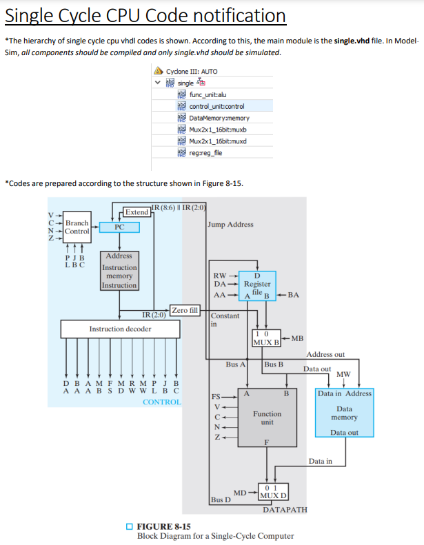
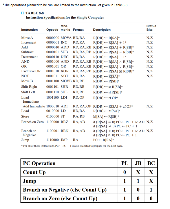
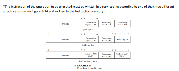
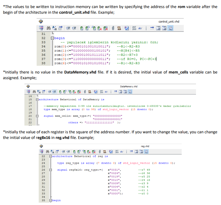
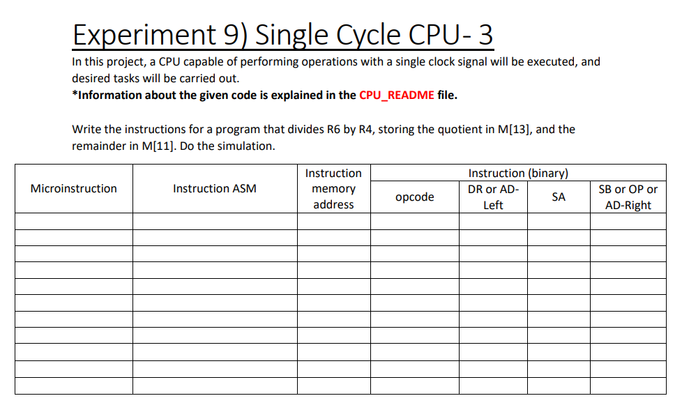
*The hierarchy of single cycle cpu vhdl codes is shown. According to this, the main module is the single.vhd file. In ModelSim, all components should be compiled and only single.vhd should be simulated. *Codes are prepared according to the structure shown in Figure 8-15. Block Diagram for a Single-Cycle Computer *The operations planned to be run, are limited to the Instruction Set given in Table 8-8. TABLE 8-8 *The Instruction of the operation to be executed must be written in binary coding according to one of the three different structures shown in Figure 8-14 and written to the Instruction memory. (a) Repsier (b) Immediale *The values to be written to instruction memory can be written by specifying the address of the rom variable after the begin of the architecture in the control_unit.vhd file. Example; *Initially there is no value in the DataMemory.vhd file. If it is desired, the initial value of mem_cells variable can be assigned. Example; *Initially the value of each register is the square of the address number. If you want to change the value, you can change the initial value of reg8x16 in reg.vhd file. Example; Experiment 9) Single Cycle CPU- 3 In this project, a CPU capable of performing operations with a single clock signal will be executed, and *Informasks will be carried out. Write the instructions for a program that divides R6 by R4, storing the quotient in M[13], and the remainder in M[11]. Do the simulation
Step by Step Solution
There are 3 Steps involved in it
Step: 1

Get Instant Access to Expert-Tailored Solutions
See step-by-step solutions with expert insights and AI powered tools for academic success
Step: 2

Step: 3
Ace Your Homework with AI
Get the answers you need in no time with our AI-driven, step-by-step assistance
Get Started
Intelligent Information And Database Systems 6th Asian Conference Aciids 2014 Bangkok Thailand April 7 9 2014 Proceedings Part I 9 2014 Proceedings Part 1 Lnai 8397
Authors: Ngoc-Thanh Nguyen ,Boonwat Attachoo ,Bogdan Trawinski ,Kulwadee Somboonviwat
2014th Edition
3319054759, 978-3319054759