

Answered step by step
Verified Expert Solution
Question
1 Approved Answer
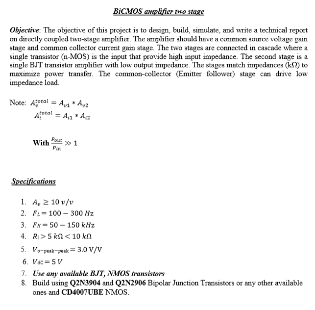
iCMOS amplifier two stage Objective: The objective of this project is to design, build, simulate, and write a technical report on directly coupled two-stage amplifier.
Step by Step Solution
There are 3 Steps involved in it
Step: 1

Get Instant Access to Expert-Tailored Solutions
See step-by-step solutions with expert insights and AI powered tools for academic success
Step: 2

Step: 3
Ace Your Homework with AI
Get the answers you need in no time with our AI-driven, step-by-step assistance
Get Started
Online Market Research Cost Effective Searching Of The Internet And Online Databases
Authors: John F. Lescher
1st Edition
0201489295, 978-0201489293