

Answered step by step
Verified Expert Solution
Question
1 Approved Answer
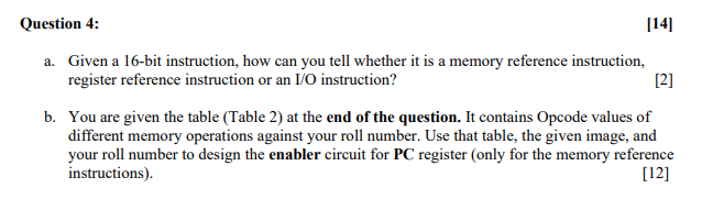
important thing- Input roll number ! 201014071 and 201014070 Question 4: [14] a. Given a 16-bit instruction, how can you tell whether it is a
important thing-
Input roll number !
201014071
and
201014070
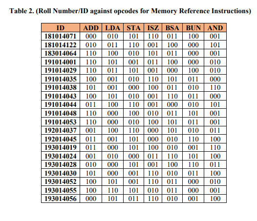
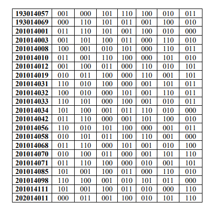
Question 4: [14] a. Given a 16-bit instruction, how can you tell whether it is a memory reference instruction, register reference instruction or an 1/0 instruction? [2] b. You are given the table (Table 2) at the end of the question. It contains Opcode values of different memory operations against your roll number. Use that table, the given image, and your roll number to design the enabler circuit for PC register (only for the memory reference instructions) [12] Image 1: Memory Reference Instructions Fetch R'To: RT: Decode RT: AR + PC IRM[AR], PC - PC + 1 DO, ..., D7 - Decode IR(12 - 14), AR-IR(0 - 11), I-IR(15) ARM[AR] Indirect D'IT: Interrupt To'T, 'T'(IEN)(FG!+ FGO): RTO: RT: R1 AR-0, TR-PC M[AR] TR, PC +0 PC - PC + 1, IENO, RO, SC 0 RT: Memory-Reference AND ADD LDA STA BUN BSA [X] TA [X] T5 [X] TA [X] T: [X] T4 [X] T5: [X] T4 [X] TA [X] TA [X] Ts: [X] TA [X] Tsi [X] TO: DR - M[AR] AC + AC A DR, SCO DR MAR] AC AC + DR, E-Cout, SC -0 DR - M[AR] AC + DR, SC 0 M[AR] - AC, SC 0 PC + AR, SCO M[AR] - PC, ARAR + 1 PC+AR, SCO DR + MAR] DR DR + 1 M[AR] - DR, if(DR=0) then (PC - PC + 1), SC_0 ISZ i. Write your roll number and the opcode values for different memory reference operations. Change the [X] to the required D value (DO, DI, ..., D7) using the opcode table provided to you at the end of the question. [2] From the image (Image 1), find out which instructions require the LD (load) enabler of PC register to be active. [2] ii. 111. From the image, find out which instructions require the CLR (clear) enabler of PC register to be active. [1] iv. From the image, find out which instructions require the INR (increment) enabler of PC register to be active. [1] V. Hence, find the overall equation for LD, CLR and INR of the DR register. [4] vi. Draw the circuit diagram using your answer to part (v). [2] 101 100 Table 2. (Roll Number/ID against opcodes for Memory Reference Instructions) ID ADD LDA STA ISZ BSA BUN AND 181014071 000 010 101 110011 100 001 181014122 010 011 110 001 100 000 183014064 110 100 010101 011 000 001 191014001 110 101 001 011 100 000 010 191014029 110 011 101 001 000 010 191014035 100 001 010110101 011 000 191014038 101 001 000 100011 010 110 191014043 100 101 010 001110 011 000 191014044 011 100 110 001 000 010 101 191014048 110 100 010011 101 001 191014053 110 010 100 101 011 001 192014037001 100 110 000 101 010 011 192014045 011 001 101 000 010 110 100 193014019 011 000 101 100 010 193014024001 010 000011 110 101 100 193014028 010 000 101 001 100 110 011 193014030 101 001110010011 100 193014052 100 101 001110011 000 193014055 100 110 101 010 011 001 193014056 000 101 011110010 001 100 000 000 001 110 000 010 000 193014057 001 193014069 000 201014001 011 201014003 001 201014008 100 201014010 011 201014012 001 201014019 010 201014031 110 201014032 100 201014033 110 201014034 101 201014042 011 201014056 110 201014058 010 201014068 011 201014070 010 201014071 011 201014085 101 201014098 110 201014111 101 202014011 000 000 101 110 100 010 110 101 011 001 100 110 101 001 100 010 101 100011 000 110 001 010 101 000 110 001 110 100 000 101 100 011 000 110 010 011 100 000 110 001 010 100 000 001 101 010 000 101 001 110 101 000 100 001 010 100 001 011 110 010 110 000 001 101 100 010 101 100 000 001 101 011 100 110 001 110 000 101 001 010 100 011 000 001 101 110 100 000 010 001 001100 011 000110 100 001 010 101 011 001 100 011 010 000 011 001 100 010 101 011 010 000 010 011 010 101 101 011 011 011 000 010 011 000 100 110 101 010 000 110 110 Question 4: [14] a. Given a 16-bit instruction, how can you tell whether it is a memory reference instruction, register reference instruction or an 1/0 instruction? [2] b. You are given the table (Table 2) at the end of the question. It contains Opcode values of different memory operations against your roll number. Use that table, the given image, and your roll number to design the enabler circuit for PC register (only for the memory reference instructions) [12] Image 1: Memory Reference Instructions Fetch R'To: RT: Decode RT: AR + PC IRM[AR], PC - PC + 1 DO, ..., D7 - Decode IR(12 - 14), AR-IR(0 - 11), I-IR(15) ARM[AR] Indirect D'IT: Interrupt To'T, 'T'(IEN)(FG!+ FGO): RTO: RT: R1 AR-0, TR-PC M[AR] TR, PC +0 PC - PC + 1, IENO, RO, SC 0 RT: Memory-Reference AND ADD LDA STA BUN BSA [X] TA [X] T5 [X] TA [X] T: [X] T4 [X] T5: [X] T4 [X] TA [X] TA [X] Ts: [X] TA [X] Tsi [X] TO: DR - M[AR] AC + AC A DR, SCO DR MAR] AC AC + DR, E-Cout, SC -0 DR - M[AR] AC + DR, SC 0 M[AR] - AC, SC 0 PC + AR, SCO M[AR] - PC, ARAR + 1 PC+AR, SCO DR + MAR] DR DR + 1 M[AR] - DR, if(DR=0) then (PC - PC + 1), SC_0 ISZ i. Write your roll number and the opcode values for different memory reference operations. Change the [X] to the required D value (DO, DI, ..., D7) using the opcode table provided to you at the end of the question. [2] From the image (Image 1), find out which instructions require the LD (load) enabler of PC register to be active. [2] ii. 111. From the image, find out which instructions require the CLR (clear) enabler of PC register to be active. [1] iv. From the image, find out which instructions require the INR (increment) enabler of PC register to be active. [1] V. Hence, find the overall equation for LD, CLR and INR of the DR register. [4] vi. Draw the circuit diagram using your answer to part (v). [2] 101 100 Table 2. (Roll Number/ID against opcodes for Memory Reference Instructions) ID ADD LDA STA ISZ BSA BUN AND 181014071 000 010 101 110011 100 001 181014122 010 011 110 001 100 000 183014064 110 100 010101 011 000 001 191014001 110 101 001 011 100 000 010 191014029 110 011 101 001 000 010 191014035 100 001 010110101 011 000 191014038 101 001 000 100011 010 110 191014043 100 101 010 001110 011 000 191014044 011 100 110 001 000 010 101 191014048 110 100 010011 101 001 191014053 110 010 100 101 011 001 192014037001 100 110 000 101 010 011 192014045 011 001 101 000 010 110 100 193014019 011 000 101 100 010 193014024001 010 000011 110 101 100 193014028 010 000 101 001 100 110 011 193014030 101 001110010011 100 193014052 100 101 001110011 000 193014055 100 110 101 010 011 001 193014056 000 101 011110010 001 100 000 000 001 110 000 010 000 193014057 001 193014069 000 201014001 011 201014003 001 201014008 100 201014010 011 201014012 001 201014019 010 201014031 110 201014032 100 201014033 110 201014034 101 201014042 011 201014056 110 201014058 010 201014068 011 201014070 010 201014071 011 201014085 101 201014098 110 201014111 101 202014011 000 000 101 110 100 010 110 101 011 001 100 110 101 001 100 010 101 100011 000 110 001 010 101 000 110 001 110 100 000 101 100 011 000 110 010 011 100 000 110 001 010 100 000 001 101 010 000 101 001 110 101 000 100 001 010 100 001 011 110 010 110 000 001 101 100 010 101 100 000 001 101 011 100 110 001 110 000 101 001 010 100 011 000 001 101 110 100 000 010 001 001100 011 000110 100 001 010 101 011 001 100 011 010 000 011 001 100 010 101 011 010 000 010 011 010 101 101 011 011 011 000 010 011 000 100 110 101 010 000 110 110Step by Step Solution
There are 3 Steps involved in it
Step: 1

Get Instant Access to Expert-Tailored Solutions
See step-by-step solutions with expert insights and AI powered tools for academic success
Step: 2

Step: 3
Ace Your Homework with AI
Get the answers you need in no time with our AI-driven, step-by-step assistance
Get Started
Learning PostgreSQL
Authors: Salahaldin Juba, Achim Vannahme, Andrey Volkov
1st Edition
178398919X, 9781783989195