Answered step by step
Verified Expert Solution
Question
1 Approved Answer
In Verilog: UDL: s2memory.v: module Mem(clk, we, in, addr, out) ; parameter n = 1, m = 1 , k = 1 DFF: module DFF(clk,
In Verilog:

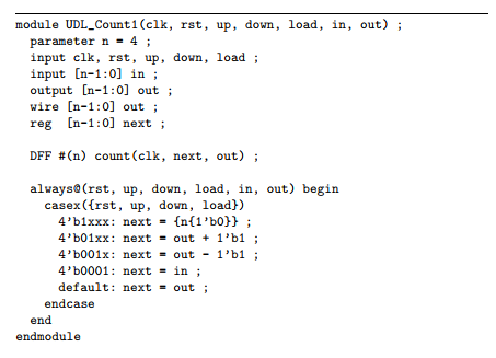
UDL:

s2memory.v:
module Mem(clk, we, in, addr, out) ; parameter n = 1, m = 1 , k = 1
DFF:
module DFF(clk, in, out) ; parameter n = 1; // width input clk ; input [n-1:0] in ; output [n-1:0] out ; reg [n-1:0] out ; always @(posedge clk) out = in ; endmodule
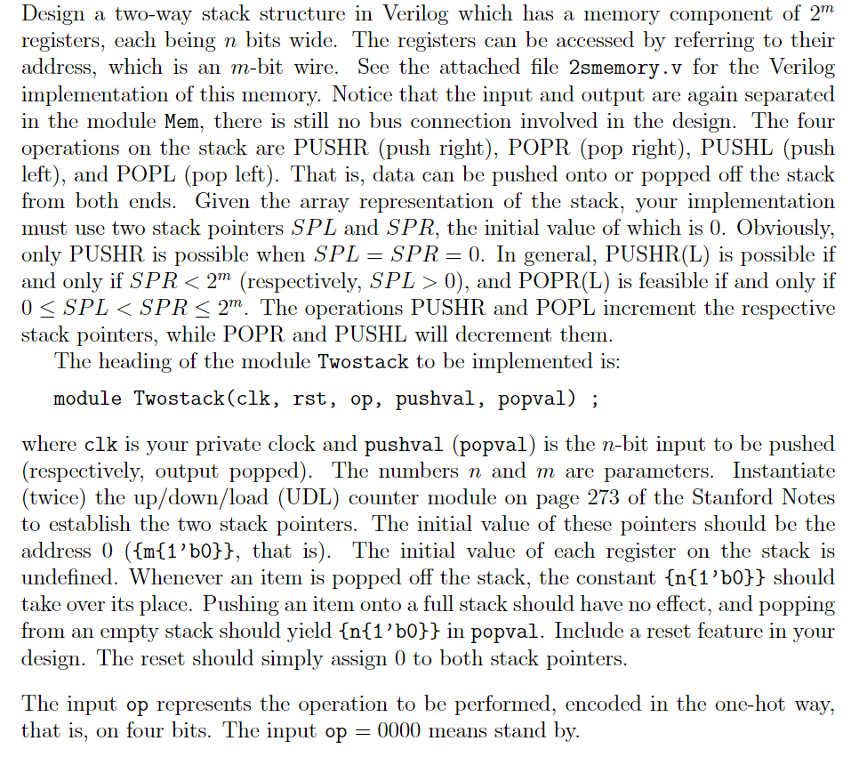
Design a two-way stack structure in Verilog which has a memory component of 2m registers, each being n bits wide. The registers can be accessed by referring to their address, which is an m-bit wire. See the attached file 2smemory.v for the Verilog implementation of this memory. Notice that the input and output are again separated in the module Mem, there is still no bus connection involved in the design. The four operations on the stack are PUSHR (push right), POPR (pop right), PUSHL (push left), and POPL (pop left). That is, data can be pushed onto or popped off the stack from both ends. Given the array representation of the stack, your implementation must use two stack pointers SPL and SPR, the initial value of which is 0. Obviously, only PUSHR is possible when SPL- SPR-0. In general, PUSHR(L) is possible if and only if SPR 0), and POPR(L) is feasible if and only if 0SPL SPR 0), and POPR(L) is feasible if and only if 0SPL SPRStep by Step Solution
There are 3 Steps involved in it
Step: 1

Get Instant Access to Expert-Tailored Solutions
See step-by-step solutions with expert insights and AI powered tools for academic success
Step: 2

Step: 3

Ace Your Homework with AI
Get the answers you need in no time with our AI-driven, step-by-step assistance
Get Started


